Japan Semiconductor Device Market Expected to Reach USD 59.7 Billion by 2033 - IMARC Group
Japan Semiconductor Device Market Statistics, Outlook and Regional Analysis 2025-2033
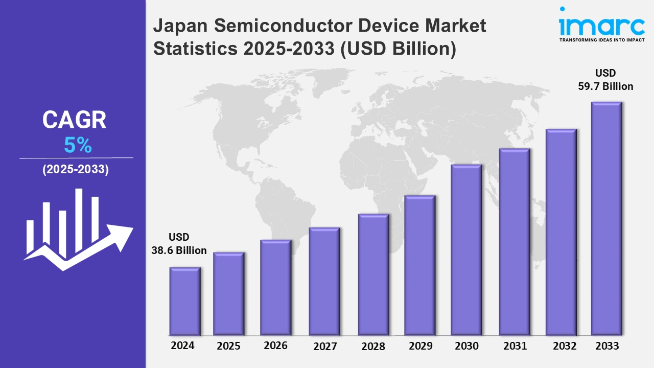
The Japan semiconductor device market size was valued at USD 38.6 Billion in 2024, and it is expected to reach USD 59.7 Billion by 2033, exhibiting a growth rate (CAGR) of 5% from 2025 to 2033.
To get more information on this market, Request Sample
The market in Japan is largely propelled by the rising integration of semiconductors in automobile technologies, continuous advances in next-generation chip development, and the extensive utilization of renewable energy systems. For example, in February 2024, Sony Semiconductor Solutions Corporation and Toyota invested around USD 20 Billion into Japan Advanced Semiconductor Manufacturing, Inc., to build a facility by the end of the 2027.
Besides this, the elevating demand for semiconductor devices across the automotive and electronics sectors is boosting the manufacturing of specialized chips for connectivity, safety, and energy efficacy, thus positively influencing the market across the country. For instance, Axcelis Technologies, Inc., the supplier of ion implantation solutions for the semiconductor industry, in June 2024, established service workplaces in Kyushu and Hokkaido to help the corps' growing consumer base. Moreover, the widespread adoption of semiconductors in IoT devices, artificial intelligence, and 5G networks, along with the expanding consumer electronics industry in Japan, is further propelling the market forward. For example, Japan-based power semiconductors creator ROHM Co. Ltd., in June 2024, launched its EcoSiC label as a trade name for derivatives using silicon carbide.
Japan Semiconductor Device Market Statistics, By Region
The market research report has also provided a comprehensive analysis of all the major regional markets, which include the Kanto region, Kansai/Kinki region, Central/ Chubu region, Kyushu-Okinawa region, Tohoku region, Chugoku region, Hokkaido region, and Shikoku region. The rising need for semiconductor devices in battery management and solar power is fueling the market expansion in Japan.
Kanto Region Semiconductor Device Market Trends:
The majority of the industry is housed in the Kanto region of Japan, primarily Tokyo and its outskirts. High-end research corporations like Sony, Toshiba, and Renesas boost the production of innovative chips and components for semiconductor devices. Moreover, Shin-Etsu Chemical Co., Ltd. (Tokyo) developed tools to manufacture semiconducting material package substrates in June 2024.
Kansai/Kinki Region Semiconductor Device Market Trends:
The market in the Kansai/Kinki region, mainly in cities like Kyoto, Osaka, and Kobe, is experiencing substantial expansion on account of the presence of high-end manufacturing plants and continuous innovation in the consumer electronics industry. Besides this, large companies like Sharp and Panasonic reside in the region, further putting a strong emphasis on semiconductor research and development. For instance, in January 2025, Mitsubishi Electric Corporation announced that in February, it will offer samples of its new module as an industrial-use energy semiconductor element for solar and other renewable power systems.
Central/Chubu Region Semiconductor Device Market Trends:
The ongoing innovations in industrial and automobile manufacturing, particularly in Nagoya prefecture, are propelling the market outlook for semiconductor devices in the Central/Chubu region. In addition to this, major players, such as Mitsubishi Electric and Denso, are among the key players in employing semiconductors in automotive systems. Furthermore, in May 2024, Toshiba completed a wafer fabrication plant for semiconductors at KagaToshiba Electronics in Ishikawa Prefecture.
Kyushu-Okinawa Region Semiconductor Device Market Trends:
The market in the Kyushu-Okinawa region of Japan is bolstering due to its massive manufacturing base as well as an increasing number of research centers and fabrication establishments. Moreover, Power Diamond Systems, a Japanese startup from Waseda University, effectively developed a technology in 2023 to improve the current-carrying capacity of diamond power devices and established an alliance with the Kyushu Institute of Technology.
Tohoku Region Semiconductor Device Market Trends:
The Tohoku region of Japan features a distinctive semiconductor device market characterized by a strong focus on cutting-edge manufacturing and research facilities. The universities and study institutes in the area are pioneers in developing advanced technologies for sustainable semiconductor production. In line with this, in September 2024, Ookuma Diamond Device, a startup derivative from Hokkaido University and the National Institute of AIST, constructed a big mass production factory in Okuma, Fukushima Prefecture.
Chugoku Region Semiconductor Device Market Trends:
The escalating number of small- and medium-sized firms specializing in electronic components is primarily driving the semiconductor device market in the Chugoku region of Japan. Besides this, the heightened emphasis of this area in forming industry collaborations and exporting and trading semiconductor derivatives to international marketplaces is also catalyzing the market reach in the region.
Hokkaido Region Semiconductor Device Market Trends:
The Hokkaido region focuses mainly on sustainability and the presence of state-of-the-art research facilities. Additionally, the cold climate in this area facilitates energy-efficient data centers, further supporting the manufacturing of high-performance semiconductors for automobile and renewable energy applications. For example, in December 2024, Rapidus Corporation, the developer of advanced logic semiconductors, installed ASML's EUV lithography equipment in its manufacturing fab in Chitose, Hokkaido.
Shikoku Region Semiconductor Device Market Trends:
The Shikoku region largely specializes in making the important elements for semiconductors. Furthermore, the presence of numerous key players involved in the manufacturing of related materials and substrates for these devices is augmenting the market expansion forward. For instance, in November 2024, Sony Semiconductor Solutions Corporation released the IMX925 arranged CMOS image instrument with back-illuminated pixel construct and shutter.
Top Companies Leading in the Japan Semiconductor Device Industry
There are several companies encompassing the semiconductor device market in Japan. For instance, in February 2025, Nuvoton Technology Corporation, Japan, unveiled its industry-leading indigo semiconductor laser, which releases an optical level of output power of 1.7W and a wavelength of 420nm. Besides this, in January 2025, Sumitomo Mitsui Banking Corporation (SMBC) launched a new finance scheme for supporting capital investment in the semiconductor manufacturing equipment sector.
Japan Semiconductor Device Market Segmentation Coverage
- Based on the device type, the market has been segmented into discrete semiconductors, optoelectronics, sensors, and integrated circuits (analog, logic, memory, and micro). Discrete semiconductors comprise standalone components like diodes and transistors. Optoelectronics contain photodiodes, solar cells, light-emitting diodes (LEDs), etc. Sensors detect and measure pressure, temperature, light, etc., while integrated circuits include numerous transistors, capacitors, and resistors.
- Based on end use vertical, the market has been categorized into automotive, communication (wired and wireless), consumer electronics, industrial, computing/data storage, and others. In the automotive sector, semiconductors are employed in EV technologies, powertrain management, etc. The communication industry uses these devices for data transmission. In consumer electronics, semiconductors power tablets, smartphones, gaming consoles, etc., they are utilized in industrial and computing/data storage to develop microchips for numerous purposes.
| Report Features | Details |
|---|---|
| Market Size in 2024 | USD 38.6 Billion |
| Market Forecast in 2033 | USD 59.7 Billion |
| Market Growth Rate 2025-2033 | 5% |
| Units | Billion USD |
| Scope of the Report | Exploration of Historical Trends and Market Outlook, Industry Catalysts and Challenges, Segment-Wise Historical and Future Market Assessment:
|
| Device Types Covered |
|
| End Use Verticals Covered | Automotive, Communication (Wired and Wireless), Consumer Electronics, Industrial, Computing/Data Storage, Others |
| Regions Covered | Kanto Region, Kansai/Kinki Region, Central/ Chubu Region, Kyushu-Okinawa Region, Tohoku Region, Chugoku Region, Hokkaido Region, Shikoku Region |
| Customization Scope | 10% Free Customization |
| Post-Sale Analyst Support | 10-12 Weeks |
| Delivery Format | PDF and Excel through Email (We can also provide the editable version of the report in PPT/Word format on special request) |
Need more help?
- Speak to our experienced analysts for insights on the current market scenarios.
- Include additional segments and countries to customize the report as per your requirement.
- Gain an unparalleled competitive advantage in your domain by understanding how to utilize the report and positively impacting your operations and revenue.
- For further assistance, please connect with our analysts.

 Inquire Before Buying
Benefits of Customization
- Personalize this research
- Triangulate with your data
- Get data as per your format and definition
- Gain a deeper dive into a specific application, geography, customer, or competitor
- Any level of personalization
 Speak to an Analyst
 Request Brochure
Get in Touch With Us
UNITED STATES
Phone: +1-201-971-6302
INDIA
Phone: +91-120-433-0800
UNITED KINGDOM
Phone: +44-753-714-6104
Email: [email protected]
Client Testimonials


.webp)