Atomic Layer Deposition Equipment Market Size, Share, Trends and Forecast by Product, Application, and Region, 2026-2034
Atomic Layer Deposition Equipment Market Size and Share:
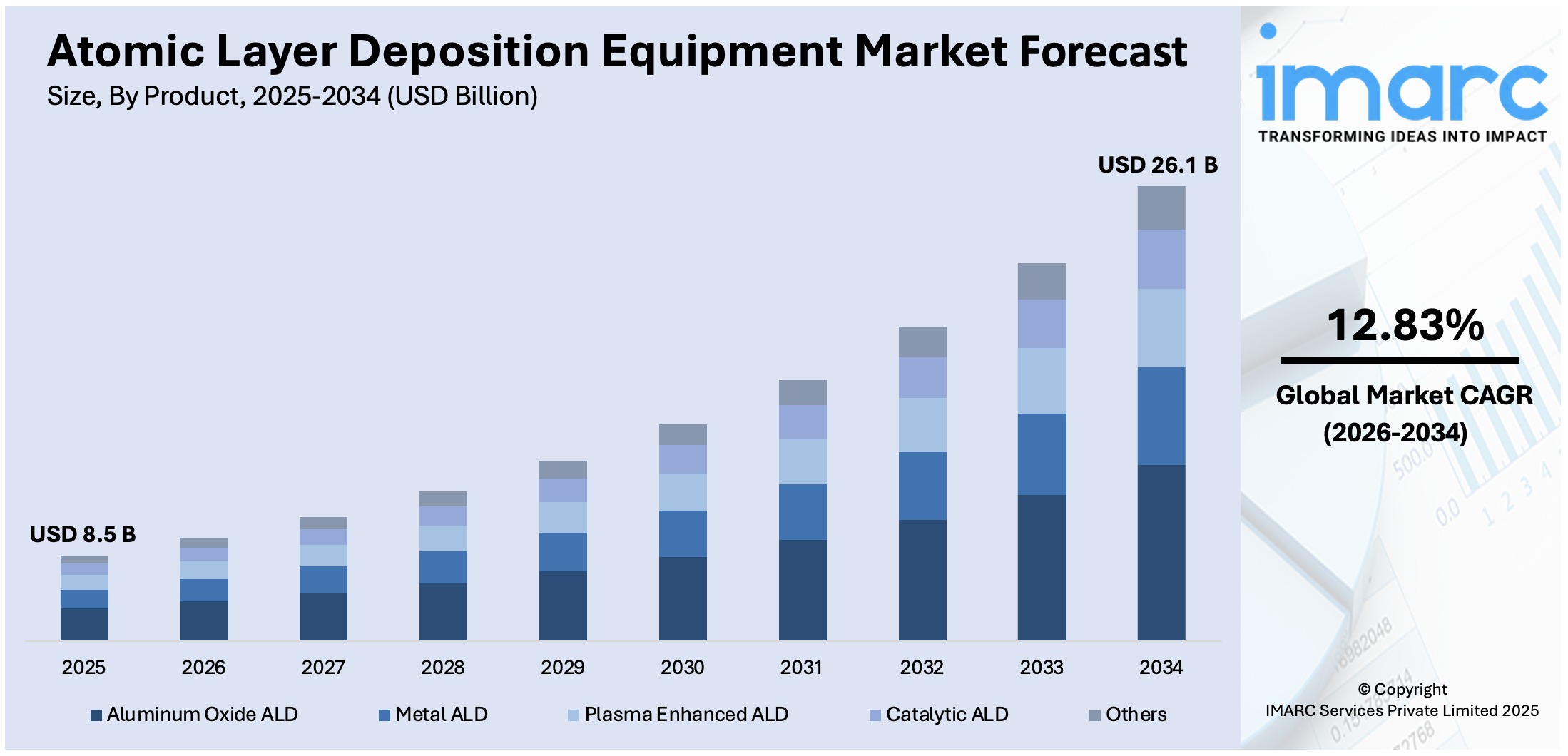
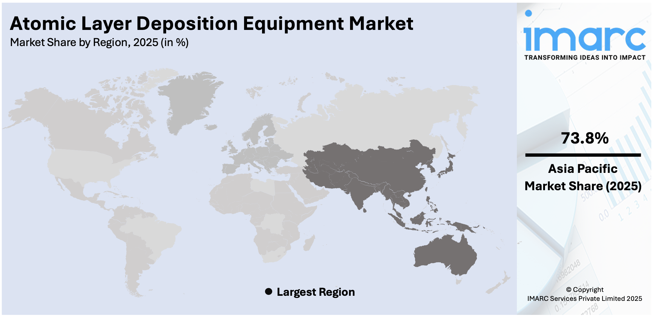
The global atomic layer deposition equipment market size was valued at USD 8.5 Billion in 2025. The market is projected to reach USD 26.1 Billion by 2034, exhibiting a CAGR of 12.83% from 2026-2034. Asia Pacific currently dominates the market, holding a market share of 73.8% in 2025. The market is driven by the increasing demand for advanced semiconductors, particularly in sub-5nm nodes where precise, conformal thin films are essential. The growth of 3D NAND and DRAM memory technologies further fuels demand, as atomic layer deposition (ALD) enables uniform coatings in high-aspect-ratio structures. Additionally, ALD’s expanding role in emerging applications such as flexible electronics, energy storage, MEMS, and biomedical devices broadens its market potential, supported by rising research and development (R&D) investments and next-generation manufacturing requirements thus strengthening the atomic layer deposition equipment market share.
|
Report Attribute
|
Key Statistics
|
|---|---|
|
Base Year
|
2025
|
|
Forecast Years
|
2026-2034
|
|
Historical Years
|
2020-2025
|
|
Market Size in 2025
|
USD 8.5 Billion |
|
Market Forecast in 2034
|
USD 26.1 Billion |
| Market Growth Rate 2026-2034 | 12.83% |
One key driver in the ALD equipment market is the rapid advancement of semiconductor technology, especially in sub-5nm nodes. As devices shrink, achieving precise, uniform, and conformal thin-film deposition becomes increasingly critical. ALD enables atomic-level control over film thickness and composition, making it essential for fabricating high-performance transistors, metal gates, and dielectrics. Its role is especially crucial in three dimenisonal (3D) architectures like FinFETs and GAAFETs, where traditional deposition techniques fall short. The continuous demand for faster, smaller, and more power-efficient chips in artificial intelligence (AI), fifth generation (5G), and consumer electronics drives widespread adoption of ALD equipment in advanced fabs.
To get more information on this market Request Sample
The U.S. plays a pivotal role in the ALD equipment market with a market share of 91.50%, driven by its leadership in semiconductor innovation and manufacturing. Major chipmakers and research institutions based in the country are pushing the boundaries of advanced nodes, requiring precise deposition technologies like ALD. Government initiatives to boost domestic semiconductor production have further accelerated investment in fabrication facilities, where ALD equipment is essential. The U.S. also benefits from a strong ecosystem of equipment suppliers, material scientists, and process engineers, fostering innovation in ALD applications. This dynamic environment positions the U.S. as a key growth region for atomic layer deposition equipment market growth.
Atomic Layer Deposition Equipment Market Trends:
Growth in 3D NAND and DRAM Memory Applications
The evolution of 3D NAND and DRAM memory technologies significantly drives the ALD equipment market. As memory architectures become increasingly complex—stacking dozens to hundreds of layers uniform deposition of ultra-thin films across high-aspect-ratio structures becomes crucial. ALD provides unmatched conformality and thickness control, making it the ideal technique for these applications. In 3D NAND, ALD is extensively used for gate oxides, spacers, and liners due to its ability to deposit high-quality films in confined spaces. DRAM scaling also benefits from ALD's precision in forming capacitors and barrier layers. The surging demand for data storage in cloud computing, mobile devices, and enterprise systems is driving investment in advanced memory fabs. This demand compels memory manufacturers to adopt ALD at scale, increasing equipment sales and fueling atomic layer deposition equipment market demand.
Expanding Applications in Emerging Technologies
Beyond semiconductors, ALD equipment is gaining traction in emerging fields like flexible electronics, microelectromechanical systems (MEMS), energy devices, and biomedical applications. For instance, ALD enables precise coatings on complex surfaces, making it suitable for encapsulating flexible OLED displays or improving the performance of lithium-ion batteries and solar cells. In MEMS, ALD is used to form dielectric and barrier layers with high uniformity, enhancing reliability and device miniaturization. Biomedical applications also benefit from ALD's biocompatible coatings and ability to modify surface properties at the nanoscale. Furthermore, industries focused on environmental sensors, wearable tech, and quantum computing are exploring ALD for its unique material engineering capabilities. As R&D investments grow and commercialization expands, the versatility of ALD across non-traditional domains opens up new revenue streams for equipment manufacturers, diversifying the market beyond traditional chipmaking.
Rising Demand for Advanced Semiconductor Devices
The global push for smaller, faster, and more energy-efficient semiconductor devices is a significant atomic layer deposition equipment market trend. As Moore’s Law pushes chipmakers toward sub-5nm nodes, traditional deposition methods fall short in terms of precision and conformity. ALD offers atomic-level thickness control and excellent step coverage, making it indispensable in fabricating high-k dielectrics, metal gates, and 3D transistor architectures like FinFETs and GAAFETs. The expansion of AI, Internet of Things (IoT), and 5G technologies increases the need for high-performance computing chips, directly benefiting the ALD sector. Additionally, the shift from planar to 3D structures in memory (like 3D NAND) and logic devices necessitates precise thin-film deposition, reinforcing ALD’s role. As foundries and integrated device manufacturers (IDMs) invest in next-gen fabrication, demand for cutting-edge ALD equipment grows, solidifying its place in advanced node manufacturing.
Atomic Layer Deposition Equipment Industry Segmentation:
IMARC Group provides an analysis of the key trends in each segment of the global atomic layer deposition equipment market, along with forecast at the global, regional, and country levels from 2026-2034. The market has been categorized based on product and application.
Analysis by Product:
- Metal ALD
- Aluminum Oxide ALD
- Plasma Enhanced ALD
- Catalytic ALD
- Others
Based on the atomic layer deposition equipment market analysis, the aluminum oxide dominates the market with a market share of 37.9% driven by its versatile properties and wide range of applications. Known for excellent dielectric strength, chemical stability, and strong barrier performance, aluminum oxide is extensively used in semiconductor manufacturing, particularly in gate oxides, passivation layers, and diffusion barriers. Its ability to form high-quality, pinhole-free films at relatively low temperatures makes it ideal for advanced logic and memory devices, as well as flexible electronics and MEMS. Additionally, it is favored in energy storage systems like lithium-ion batteries and solar cells for surface protection and performance enhancement. The material’s compatibility with various substrates and processes ensures its continued dominance in both mature and emerging ALD applications across industries.
Analysis by Application:
Access the comprehensive market breakdown Request Sample
- Semiconductors
- Solar Devices
- Electronics
- Medical Equipment
- Others
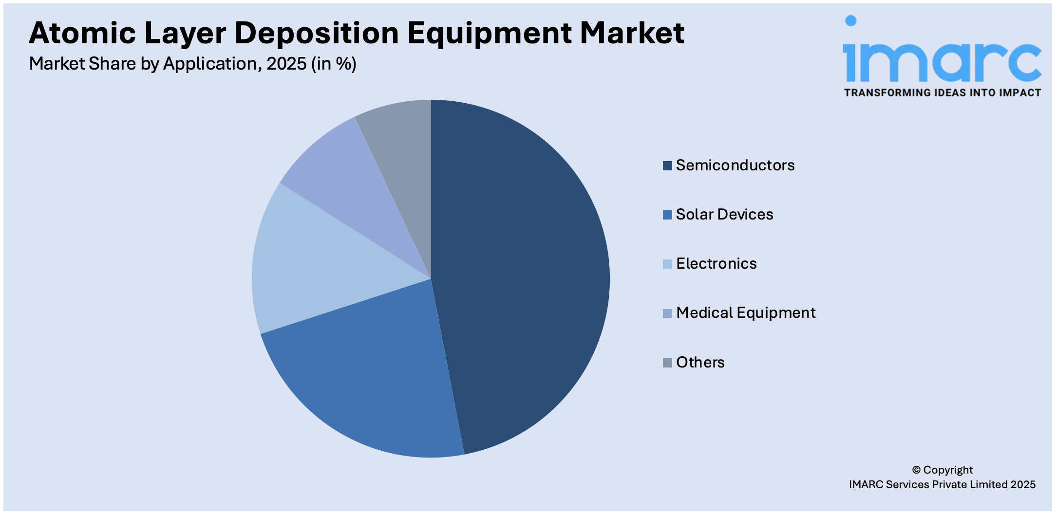
Semiconductors account for the majority of shares of 46.7% owing to their critical need for precise and conformal thin-film deposition. As chip designs move toward smaller nodes and complex 3D architectures like FinFETs and 3D NAND, ALD becomes essential for achieving atomic-level thickness control, excellent step coverage, and high material quality. It is widely used in depositing high-k dielectrics, metal gates, spacers, and barrier layers—key components in modern integrated circuits. The continuous demand for faster, smaller, and more power-efficient chips across smartphones, data centers, AI, and IoT devices reinforces ALD’s role in semiconductor fabrication. As a result, the semiconductor sector remains the primary driver of ALD equipment adoption, securing the largest market share in the atomic layer deposition equipment market forecast.
Regional Analysis:
To get more information on the regional analysis of this market Request Sample
- North America
- United States
- Canada
- Asia Pacific
- China
- Japan
- India
- South Korea
- Australia
- Indonesia
- Others
- Europe
- Germany
- France
- United Kingdom
- Italy
- Spain
- Russia
- Others
- Latin America
- Brazil
- Mexico
- Others
- Middle East and Africa
Asia Pacific is the leading region with a market share of 73.8% due to its strong presence of semiconductor manufacturing hubs, especially in countries like China, South Korea, Taiwan, and Japan. These nations house major foundries and memory producers that drive high-volume demand for ALD systems in advanced logic and memory chip fabrication. Additionally, supportive government policies, increasing investment in new fabs, and the rapid growth of consumer electronics, 5G, and electric vehicles contribute to market expansion. The region also benefits from a well-developed supply chain, skilled workforce, and continuous R&D in nanotechnology and materials science. This ecosystem enables Asia Pacific to maintain its leadership in both ALD equipment production and consumption across various high-tech industries.
Key Regional Takeaways:
North America Atomic Layer Deposition Equipment Market Analysis
The North America Atomic Layer Deposition (ALD) equipment market is witnessing significant growth driven by increasing demand in semiconductor manufacturing, advanced electronics, and nanotechnology applications. ALD technology enables precise, atomic-scale deposition of thin films, which is critical for producing high-performance and miniaturized electronic components. The rising adoption of 3D NAND, FinFET technologies, and next-generation memory solutions has accelerated the need for ALD systems across the region. The United States leads the market, supported by the presence of major semiconductor fabs, strong R&D infrastructure, and government initiatives promoting domestic chip production. Additionally, the growing use of ALD in emerging sectors like solar photovoltaics, flexible electronics, and medical devices is further boosting market expansion. Key players such as Applied Materials, Lam Research, and Veeco Instruments dominate the landscape with continual innovation and strategic partnerships. Challenges include high equipment costs and technical complexities, but ongoing advancements in ALD process integration are expected to overcome these hurdles. Overall, the North American ALD equipment market is poised for robust growth through 2030.
United States Atomic Layer Deposition Equipment Market Analysis
The United States atomic layer deposition equipment market is primarily driven by the increasing need for ultra-thin, conformal films, which are essential in advanced semiconductor node scaling. In accordance with this, the growing adoption of chipset-based architectures and heterogeneous integration is propelling market growth. The ongoing implementation of federal initiatives, including the CHIPS Act, is bolstering domestic semiconductor manufacturing capacity and fueling ALD equipment procurement. Similarly, the expansion of silicon photonics for data communication and optical computing is accelerating the uptake of specialized deposition tools. As such, in October 2024, AIM Photonics received USD 321 Million under a seven-year agreement to advance U.S. silicon photonics manufacturing, supporting defense and microelectronics applications critical to national security and high-performance technology development. The rising focus on defect reduction and yield optimization in high-volume fabs is further enhancing market appeal. Additionally, the rapid integration of compound semiconductors in RF and power electronics, which reinforces the relevance of ALD processes, is fostering market expansion. Apart from this, increasing interest in modular and customizable ALD platforms is shaping buyer preferences and creating lucrative opportunities in the market.
Europe Atomic Layer Deposition Equipment Market Analysis
The market in Europe is experiencing growth due to increasing investments in semiconductor sovereignty initiatives, notably under the European Chips Act. As such, in March 2025, nine European countries formed the Semicon Coalition to augment the EU semiconductor sector, aligning efforts on strategy with EUR 43 Billion in funding under the EU Chips Act. In line with this, the rising demand for ALD in quantum computing research is driving the need for precise thin-film deposition tools. Similarly, expanding applications of ALD in photonics and optical technologies, especially in autonomous systems and high-speed data transmission, are supporting market growth. The growing need for biocompatible coatings in wearable medical devices and diagnostics is enhancing market appeal. Furthermore, the ongoing electrification of transportation and the demand for reliable power components in electric vehicles, driving increased usage in automotive applications, is impelling the market. Additionally, numerous academic-industry collaborations that foster innovation in deposition methods are strengthening market demand. Besides this, stringent EU sustainability regulations are increasing reliance on resource-efficient, precision manufacturing solutions, such as atomic layer deposition (ALD), thereby expanding the market scope.
Asia Pacific Atomic Layer Deposition Equipment Market Analysis
The Asia Pacific market is largely propelled by the region’s leadership in semiconductor manufacturing, with countries such as South Korea, Taiwan, and China hosting several of the world’s largest foundries. In addition to this, the rise in memory chip production and investments in fabrication facilities is significantly supporting market demand. The rising consumption of smartphones, tablets, and wearables, which drive demand for miniaturized components, is driving market expansion. A recent MoSPI survey showed over 85% of Indian households own smartphones, with ownership among young adults aged 15–29 approaching universal levels. Similarly, countries across the region are increasing their research and development (R&D) spending on nanomaterials and surface engineering to maintain market competitiveness. Moreover, the rapid integration of ALD in OLED and microLED displays is gaining traction in the market due to the growing demand for high-performance displays. Furthermore, the rapid growth of the electric vehicle industry is accelerating the adoption of ALD tools for enhancing battery performance and improving thermal stability.
Latin America Atomic Layer Deposition Equipment Market Analysis
In Latin America, the atomic layer deposition equipment market is growing due to rising investments in semiconductor research, particularly in Brazil and Mexico, aimed at strengthening regional technological capabilities. Similarly, the expansion of academic and industrial collaboration driving innovation in thin-film applications for sensors and optoelectronic devices is expanding the market reach. Furthermore, the growing demand for advanced medical devices is encouraging the use of ALD for biocompatible coatings. Moreover, the region’s increasing focus on renewable energy, driving the adoption of photovoltaic cell development, is providing an impetus to the market. In 2024, 88% of Brazil’s electricity came from renewable sources, with wind and solar accounting for approximately 24% of total demand, according to data from state energy agency Empresa de Pesquisa Energetica (EPE).
Middle East and Africa Atomic Layer Deposition Equipment Market Analysis
The market in the Middle East and Africa is significantly influenced by rising investments in semiconductor manufacturing, particularly in Gulf countries seeking economic diversification beyond oil. Accordingly, in October 2024, Samsung and TSMC began talks with the UAE to build chip plants worth over USD 100 Billion amid the UAE's push to become a global tech hub with U.S. cooperation. Furthermore, increasing demand for high-precision electronics in aerospace, defense, and telecommunications is supporting the adoption of atomic layer deposition technologies. Additionally, the establishment of nanotechnology research centers and academic initiatives across the region is promoting market accessibility. Besides this, growing interest in solar energy development, especially in North African nations, is accelerating the use of ALD equipment in photovoltaic cell production and related renewable technologies.

Competitive Landscape:
The competitive landscape is shaped by rapid technological advancements and the growing demand for high-precision thin-film deposition across various industries. Players in the market compete on innovation, process control, deposition speed, and equipment scalability to meet evolving semiconductor and emerging application needs. The shift toward advanced nodes and three dimensional (3D) architectures intensifies the need for highly reliable and customizable ALD tools. Additionally, companies are investing in R&D to enhance film quality, reduce cycle times, and expand material compatibility. Strategic partnerships with foundries, research institutes, and materials providers are also common, fostering co-development of next-generation solutions. The market is moderately consolidated, with a few dominant players and a growing number of niche entrants targeting specific applications such as flexible electronics and energy devices. Regulatory compliance, service support, and global distribution capabilities further influence competitiveness.
The report provides a comprehensive analysis of the competitive landscape in the atomic layer deposition equipment market with detailed profiles of all major companies, including:
- ANRIC Technologies
- Applied Materials, Inc.
- Arradiance LLC
- ASM International N.V.
- Beneq
- Forge Nano Inc.
- Lam Research Corporation
- NCD Co. Ltd.
- Oxford Instruments
- SENTECH Instruments GmbH
- The Kurt J. Lesker Company
- Tokyo Electron Limited
- Veeco Instruments Inc
Latest News and Developments:
- February 2025: Lam Research launched ALTUS Halo, the first ALD tool enabling high-volume molybdenum deposition for advanced semiconductors. Targeting 3D NAND, DRAM, and logic, it offers lower resistivity than tungsten, eliminates barrier layers, and supports faster chip performance. ALTUS Halo is already in use at leading fabs.
- January 2025: Forge Nano opened a 2,000 sq/ft Class 10 cleanroom to triple production of its TEPHRA ALD tools for 200mm semiconductor wafers. The facility supports high-throughput single-wafer processing, tool demos, and advanced metrology, targeting applications in advanced packaging, MEMS, RF devices, and 3D chip integration.
- November 2024: 2D Generation ordered a specialized ALD machine from Beneq to support its next-gen semiconductor development, including graphene-coated interconnects. Funded by Adisyn, the machine will be installed in 5–6 months. It supports 200 mm wafers, plasma processing, and high temperatures, enhancing 2DG’s chip innovation capabilities.
- August 2024: Kalpana Systems, a Dutch company, introduced roll-to-roll spatial atomic layer deposition (sALD) tools aimed at the solar PV, OLED, battery, and packaging sectors. The tools are designed for barrier layer applications. Two models, K300 and K600, support high-speed industrial coating with flexible integration.
- July 2024: Finland-based Chipmetrics launched two new semiconductor test chips: PillarHall LHAR5 for high aspect ratio ALD process monitoring, and ASD-1 for Area Selective Deposition (ASD) prototyping. Both are compatible with 300 mm tools, supporting advanced metrology in 3D NAND, DRAM, and miniaturized device manufacturing.
- July 2024: Forge Nano launched TEPHRA, a high-throughput single-wafer ALD cluster tool for 200mm semiconductor wafers. Designed for advanced packaging and MEMS, TEPHRA supports high aspect ratio coatings with efficient chemical use. It features multiple deposition chambers and operates between 80–300°C using Forge Nano’s ALDx and CRISP technologies.
Atomic Layer Deposition Equipment Market Report Scope:
| Report Features | Details |
|---|---|
| Base Year of the Analysis | 2025 |
| Historical Period | 2020-2025 |
| Forecast Period | 2026-2034 |
| Units | Billion USD |
| Scope of the Report |
Exploration of Historical Trends and Market Outlook, Industry Catalysts and Challenges, Segment-Wise Historical and Future Market Assessment:
|
| Products Covered | Metal ALD, Aluminum Oxide ALD, Plasma Enhanced ALD, Catalytic ALD, Others |
| Applications Covered | Semiconductors, Solar Devices, Electronics, Medical Equipment, Others |
| Regions Covered | Asia Pacific, Europe, North America, Latin America, Middle East and Africa |
| Countries Covered | United States, Canada, Germany, France, United Kingdom, Italy, Spain, Russia, China, Japan, India, South Korea, Australia, Indonesia, Brazil, Mexico |
| Companies Covered | ANRIC Technologies, Applied Materials, Inc., Arradiance LLC, ASM International N.V., Beneq, Forge Nano Inc., Lam Research Corporation, NCD Co. Ltd., Oxford Instruments, SENTECH Instruments GmbH, The Kurt J. Lesker Company, Tokyo Electron Limited, Veeco Instruments Inc, etc. |
| Customization Scope | 10% Free Customization |
| Post-Sale Analyst Support | 10-12 Weeks |
| Delivery Format | PDF and Excel through Email (We can also provide the editable version of the report in PPT/Word format on special request) |
Key Benefits for Stakeholders:
- IMARC’s report offers a comprehensive quantitative analysis of various market segments, historical and current market trends, market forecasts, and dynamics of the atomic layer deposition equipment market from 2020-2034.
- The research study provides the latest information on the market drivers, challenges, and opportunities in the global atomic layer deposition equipment market.
- The study maps the leading, as well as the fastest-growing, regional markets. It further enables stakeholders to identify the key country-level markets within each region.
- Porter's Five Forces analysis assists stakeholders in assessing the impact of new entrants, competitive rivalry, supplier power, buyer power, and the threat of substitution. It helps stakeholders to analyze the level of competition within the atomic layer deposition equipment industry and its attractiveness.
- Competitive landscape allows stakeholders to understand their competitive environment and provides an insight into the current positions of key players in the market.
Frequently Asked Questions About the Atomic Layer Deposition Equipment Market Report
The atomic layer deposition equipment market was valued at USD 8.5 Billion in 2025.
The atomic layer deposition equipment market is projected to exhibit a CAGR of 12.83% during 2026-2034, reaching a value of USD 26.1 Billion by 2034.
Key factors driving the atomic layer deposition equipment market include the demand for advanced semiconductor nodes, growth in 3D NAND and DRAM technologies, and increasing adoption in emerging applications like flexible electronics, energy storage, and MEMS. ALD’s precision, conformality, and material versatility make it essential for next-generation device fabrication.
Asia Pacific currently dominates the atomic layer deposition equipment market, accounting for a share of 73.8% owing to its concentration of leading semiconductor manufacturers, robust electronics production, and significant investments in advanced fabrication facilities. Supportive government policies and strong regional demand for consumer electronics further reinforce its market leadership.
Some of the major players in the atomic layer deposition equipment market include ANRIC Technologies, Applied Materials, Inc., Arradiance LLC, ASM International N.V., Beneq, Forge Nano Inc., Lam Research Corporation, NCD Co. Ltd., Oxford Instruments, SENTECH Instruments GmbH, The Kurt J. Lesker Company, Tokyo Electron Limited, and Veeco Instruments Inc, etc.
Need more help?
- Speak to our experienced analysts for insights on the current market scenarios.
- Include additional segments and countries to customize the report as per your requirement.
- Gain an unparalleled competitive advantage in your domain by understanding how to utilize the report and positively impacting your operations and revenue.
- For further assistance, please connect with our analysts.
 Request Customization
 Speak to an Analyst
 Request Brochure
 Inquire Before Buying
Benefits of Customization
- Personalize this research
- Triangulate with your data
- Get data as per your format and definition
- Gain a deeper dive into a specific application, geography, customer, or competitor
- Any level of personalization
Get in Touch With Us
UNITED STATES
Phone: +1-201-971-6302
INDIA
Phone: +91-120-433-0800
UNITED KINGDOM
Phone: +44-753-714-6104
Email: [email protected]
Client Testimonials

.webp)