India Semiconductor Packaging Market Size, Share, Trends, and Forecast by Type, Packaging Material, Technology, End User, and Region, 2025-2033
India Semiconductor Packaging Market Overview:
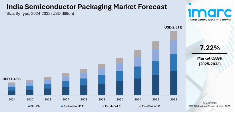
The India semiconductor packaging market size reached USD 1.43 Billion in 2024. Looking forward, IMARC Group expects the market to reach USD 2.81 Billion by 2033, exhibiting a growth rate (CAGR) of 7.22% during 2025-2033. The market is expanding rapidly, driven by government initiatives like the India Semiconductor Mission (ISM) and Production Linked Incentive (PLI) scheme. Additionally, investments from global players, advancements in 2.5D, 3D ICs, and System-in-Package (SiP) technologies, and the rising demand in consumer electronics and automotive sectors are strengthening domestic packaging capabilities and supply chains.
|
Report Attribute
|
Key Statistics
|
|---|---|
|
Base Year
|
2024 |
|
Forecast Years
|
2025-2033
|
|
Historical Years
|
2019-2024
|
| Market Size in 2024 | USD 1.43 Billion |
| Market Forecast in 2033 | USD 2.81 Billion |
| Market Growth Rate 2025-2033 | 7.22% |
India Semiconductor Packaging Market Trends:
Government Support and Local Manufacturing Expansion
India's semiconductor packaging market is experiencing rapid growth due to strong government support and increasing local manufacturing efforts. The India Semiconductor Mission (ISM) is attracting global players with financial incentives and policy support, fostering domestic chip packaging and assembly capabilities. The Production Linked Incentive (PLI) scheme further encourages investment in semiconductor manufacturing, strengthening India’s position in the global supply chain. For instance, in September 2024, NXP Semiconductors announced plans to invest USD 1 Billion in India to expand research and development (R&D). This investment strengthens India's semiconductor packaging capabilities, enhancing its role in the global supply chain. These initiatives align with India's goal of becoming a semiconductor hub, ensuring a stable supply chain for consumer electronics and automotive industries. The push for localization is also driving collaborations between global semiconductor firms and Indian technology companies to develop high-quality packaging solutions.
To get more information on this market, Request Sample
Advancements in Packaging Technologies
The Indian semiconductor packaging industry is shifting towards advanced packaging technologies such as 2.5D, 3D ICs, and System-in-Package (SiP) solutions. For instance, in August 2024, Kaynes SemiCon announced an MoU with Lightspeed Photonics, securing India’s first paying OSAT customer. The partnership enables Kaynes to provide advanced packaging for Lightspeed’s LightSiP technology, enhancing semiconductor manufacturing and supporting high-volume production in India’s growing semiconductor ecosystem. These technologies enhance chip performance, power efficiency, and miniaturization, catering to the growing demand for high-performance computing, artificial intelligence, and IoT applications. With increasing adoption of 5G, electric vehicles, and smart devices, semiconductor firms in India are investing in research and development to improve packaging capabilities. Furthermore, this trend is crucial for India's semiconductor ecosystem, helping local manufacturers meet international quality standards while addressing the increasing complexity of modern semiconductor applications.
India Semiconductor Packaging Market Segmentation:
IMARC Group provides an analysis of the key trends in each segment of the market, along with forecasts at the region level for 2025-2033. Our report has categorized the market based on type, packaging material, technology, and end user.
Type Insights:
- Flip Chip
- Embedded DIE
- Fan-In WLP
- Fan-Out WLP
The report has provided a detailed breakup and analysis of the market based on the type. This includes flip chip, embedded DIE, fan-in WLP, and fan-out WLP.
Packaging Material Insights:
- Organic Substrate
- Bonding Wire
- Leadframe
- Ceramic Package
- Die Attach Material
- Others
A detailed breakup and analysis of the market based on the packaging material have also been provided in the report. This includes organic substrate, bonding wire, leadframe, ceramic package, die attach material, and others.
Technology Insights:
- Grid Array
- Small Outline Package
- Flat No-Leads Package
- Dual In-Line Package
- Others
The report has provided a detailed breakup and analysis of the market based on the technology. This includes grid array, small outline package, flat no-leads package, dual in-line package, and others.
End User Insights:
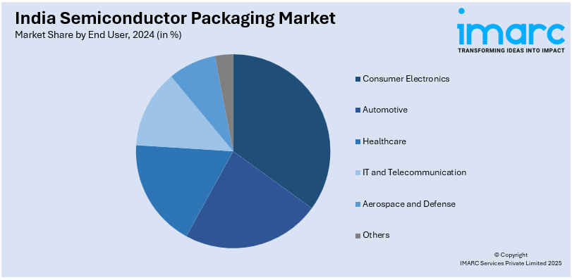
- Consumer Electronics
- Automotive
- Healthcare
- IT and Telecommunication
- Aerospace and Defense
- Others
A detailed breakup and analysis of the market based on the end user have also been provided in the report. This includes consumer electronics, automotive, healthcare, IT and telecommunication, aerospace and defense, and others.
Regional Insights:
- North India
- South India
- East India
- West India
The report has also provided a comprehensive analysis of all the major regional markets, which include North India, South India, East India, and West India.
Competitive Landscape:
The market research report has also provided a comprehensive analysis of the competitive landscape. Competitive analysis such as market structure, key player positioning, top winning strategies, competitive dashboard, and company evaluation quadrant has been covered in the report. Also, detailed profiles of all major companies have been provided.
India Semiconductor Packaging Market News:
- In September 2024, the Government of India (GOI) announced the approval of a proposal by Kaynes Semicon to set up a semiconductor unit in Sanand, Gujarat, with an investment of INR 33.07 billion (approximately US$394.15 million). This facility will enhance domestic semiconductor packaging and testing capacities, catering to automotive, consumer electronics, and telecommunications sectors.
India Semiconductor Packaging Market Report Coverage:
| Report Features | Details |
|---|---|
| Base Year of the Analysis | 2024 |
| Historical Period | 2019-2024 |
| Forecast Period | 2025-2033 |
| Units | Billion USD |
| Scope of the Report | Exploration of Historical Trends and Market Outlook, Industry Catalysts and Challenges, Segment-Wise Historical and Future Market Assessment:
|
| Types Covered | Flip Chip, Embedded DIE, Fan-In WLP, Fan-Out WLP |
| Packaging Materials Covered | Organic Substrate, Bonding Wire, Leadframe, Ceramic Package, Die Attach Material, Others |
| Technologies Covered | Grid Array, Small Outline Package, Flat No-Leads Package, Dual In-Line Package, Others |
| End Users Covered | Consumer Electronics, Automotive, Healthcare, IT and Telecommunication, Aerospace and Defense, Others |
| Regions Covered | North India, South India, East India, West India |
| Customization Scope | 10% Free Customization |
| Post-Sale Analyst Support | 10-12 Weeks |
| Delivery Format | PDF and Excel through Email (We can also provide the editable version of the report in PPT/Word format on special request) |
Key Questions Answered in This Report:
- How has the India semiconductor packaging market performed so far and how will it perform in the coming years?
- What is the breakup of the India semiconductor packaging market on the basis of type?
- What is the breakup of the India semiconductor packaging market on the basis of packaging material?
- What is the breakup of the India semiconductor packaging market on the basis of technology?
- What is the breakup of the India semiconductor packaging market on the basis of end user?
- What is the breakup of the India semiconductor packaging market on the basis of region?
- What are the various stages in the value chain of the India semiconductor packaging market?
- What are the key driving factors and challenges in the India semiconductor packaging market?
- What is the structure of the India semiconductor packaging market and who are the key players?
- What is the degree of competition in the India semiconductor packaging market?
Key Benefits for Stakeholders:
- IMARC’s industry report offers a comprehensive quantitative analysis of various market segments, historical and current market trends, market forecasts, and dynamics of the India semiconductor packaging market from 2019-2033.
- The research report provides the latest information on the market drivers, challenges, and opportunities in the India semiconductor packaging market.
- Porter's five forces analysis assist stakeholders in assessing the impact of new entrants, competitive rivalry, supplier power, buyer power, and the threat of substitution. It helps stakeholders to analyze the level of competition within the India semiconductor packaging industry and its attractiveness.
- Competitive landscape allows stakeholders to understand their competitive environment and provides an insight into the current positions of key players in the market.
Need more help?
- Speak to our experienced analysts for insights on the current market scenarios.
- Include additional segments and countries to customize the report as per your requirement.
- Gain an unparalleled competitive advantage in your domain by understanding how to utilize the report and positively impacting your operations and revenue.
- For further assistance, please connect with our analysts.
 Request Customization
 Speak to an Analyst
 Request Brochure
 Inquire Before Buying
Benefits of Customization
- Personalize this research
- Triangulate with your data
- Get data as per your format and definition
- Gain a deeper dive into a specific application, geography, customer, or competitor
- Any level of personalization
Get in Touch With Us
UNITED STATES
Phone: +1-201-971-6302
INDIA
Phone: +91-120-433-0800
UNITED KINGDOM
Phone: +44-753-714-6104
Email: sales@imarcgroup.com
Client Testimonials
.webp)