Japan Semiconductor Packaging Market Size, Share, Trends and Forecast by Type, Packaging Material, Technology, End User, and Region, 2026-2034
Japan Semiconductor Packaging Market Overview:
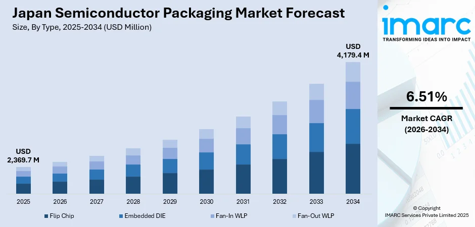
The Japan semiconductor packaging market size reached USD 2,369.7 Million in 2025. Looking forward, IMARC Group expects the market to reach USD 4,179.4 Million by 2034, exhibiting a growth rate (CAGR) of 6.51% during 2026-2034. The market is driven by rising demand for compact, high-performance consumer electronics, advancements in automotive electronics, and increased deployment of AI and 5G technologies. Government support for domestic chip production and strong R&D investments by local manufacturers also contribute to growth, ensuring technological competitiveness and supply chain resilience.
|
Report Attribute
|
Key Statistics
|
|---|---|
|
Base Year
|
2025 |
|
Forecast Years
|
2026-2034
|
|
Historical Years
|
2020-2025
|
| Market Size in 2025 | USD 2,369.7 Million |
| Market Forecast in 2034 | USD 4,179.4 Million |
| Market Growth Rate 2026-2034 | 6.51% |
Japan Semiconductor Packaging Market Trends:
Integration of Advanced Automotive Electronics
Japan’s prominence in automotive innovation is significantly influencing its semiconductor packaging landscape. As electric vehicles (EVs), autonomous systems, and connected car technologies become more sophisticated, demand is rising for robust semiconductor packages that can withstand high thermal loads and complex functionality. Japanese automakers are increasingly incorporating advanced driver-assistance systems (ADAS), power modules, and in-vehicle infotainment—each requiring compact and high-reliability semiconductor packaging. This shift is pushing packaging providers to develop heat-resistant and space-efficient solutions, such as multi-chip modules and system-in-package (SiP) configurations. Collaborations between semiconductor firms and automotive OEMs have accelerated, focusing on vertical integration and co-development of packaging technologies tailored to vehicular environments. The convergence of automotive and semiconductor sectors is thus reshaping packaging priorities, with emphasis on longevity, precision, and miniaturization. For instance, in December 2024, TOPPAN Inc. announced its participation in the US-JOINT consortium, a U.S.-Japan initiative led by Resonac Corporation to develop next-generation semiconductor packaging technologies. TOPPAN will contribute as a packaging substrate manufacturer, supporting advancements in 2.5D and 3D packaging for applications like AI and autonomous driving.
To get more information on this market Request Sample
Rise of Glass Core Substrates in High-Density Packaging
Japan is witnessing growing interest in the adoption of glass core substrates for high-density semiconductor packaging, particularly for applications in data centers, AI chips, and high-performance computing. Glass substrates offer superior dimensional stability, better electrical insulation, and flatter surfaces compared to traditional organic materials, enabling more precise layering and interconnect density. Japanese companies are investing in refining the fabrication processes for glass-based substrates to enhance yield and integration capability. This trend aligns with global shifts toward chiplet architectures, where multiple smaller chips are integrated on a single substrate to function as a unified system. Japanese firms, known for their material science expertise, are uniquely positioned to lead innovations in this domain, helping meet performance, space, and power efficiency requirements of emerging computing platforms. For instance, in June 2024, Rapidus Corporation and IBM announced an expanded partnership focused on developing chiplet packaging technologies for 2nm-generation semiconductors. Building on an existing 2nm node collaboration, the initiative is part of a NEDO-backed Japanese project to advance next-gen semiconductor packaging. The goal is to establish Japan as a key player in advanced chiplet packaging, supporting AI and HPC applications and strengthening the global semiconductor supply chain.
Japan Semiconductor Packaging Market Segmentation:
IMARC Group provides an analysis of the key trends in each segment of the market, along with forecasts at the country and regional levels for 2026-2034. Our report has categorized the market based on type, packaging material, technology, and end user.
Type Insights:
- Flip Chip
- Embedded DIE
- Fan-In WLP
- Fan-Out WLP
The report has provided a detailed breakup and analysis of the market based on the type. This includes flip chip, embedded DIE, fan-in WLP, and fan-out WLP.
Packaging Material Insights:
- Organic Substrate
- Bonding Wire
- Leadframe
- Ceramic Package
- Die Attach Material
- Others
A detailed breakup and analysis of the market based on the packaging material have also been provided in the report. This includes organic substrate, bonding wire, leadframe, ceramic package, die attach material, and others.
Technology Insights:
- Grid Array
- Small Outline Package
- Flat no-leads Package
- Dual In-Line Package
- Others
The report has provided a detailed breakup and analysis of the market based on the technology. This includes grid array, small outline package, flat no-leads package, dual in-line package, and others.
End User Insights:
Access the comprehensive market breakdown Request Sample
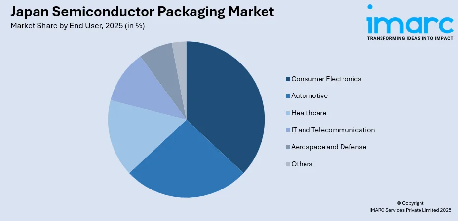
- Consumer Electronics
- Automotive
- Healthcare
- IT and Telecommunication
- Aerospace and Defense
- Others
A detailed breakup and analysis of the market based on the end user have also been provided in the report. This includes consumer electronics, automotive, healthcare, IT and telecommunication, aerospace and defense, and others.
Regional Insights:
- Kanto Region
- Kansai/Kinki Region
- Central/ Chubu Region
- Kyushu-Okinawa Region
- Tohoku Region
- Chugoku Region
- Hokkaido Region
- Shikoku Region
The report has also provided a comprehensive analysis of all the major regional markets, which include Kanto, Kansai/Kinki, Central/ Chubu, Kyushu-Okinawa, Tohoku, Chugoku, Hokkaido, and Shikoku Region.
Competitive Landscape:
The market research report has also provided a comprehensive analysis of the competitive landscape. Competitive analysis such as market structure, key player positioning, top winning strategies, competitive dashboard, and company evaluation quadrant has been covered in the report. Also, detailed profiles of all major companies have been provided.
Japan Semiconductor Packaging Market News:
- In February 2025, PanelSemi entered into a memorandum of understanding with Japan Display Inc. (JDI) to collaborate on the development of ceramic semiconductor packaging technologies. The initiative targets next-generation ceramic substrates, recognized for their superior thermal performance, durability, and suitability for integrated semiconductor use. Through this partnership, the two companies aim to reinforce Japan’s role in the global semiconductor packaging landscape, with a focus on advancing panel-level and high-performance packaging capabilities.
- In October 2024, SEMIFIVE, a leading platform-based SoC design solution provider, signed a Memorandum of Understanding (MOU) with Japan’s MegaChips, a pioneer in fabless system LSI manufacturing. The partnership aims to collaborate on semiconductor design, seek new customer opportunities in Japan, and provide on-site technical support. SEMIFIVE, known for its AI-focused SoC platforms, will leverage its design expertise to complement MegaChips’ advanced ASIC and ASSP capabilities. This collaboration strengthens SEMIFIVE’s position in Japan’s semiconductor ecosystem and supports the growing demand for custom silicon solutions across AI and high-performance applications.
- In July 2024, Resonac announced the launch of the US-JOINT alliance, a collaboration between leading semiconductor firms from Japan and the United States to advance next-generation semiconductor packaging. Japanese participants include Resonac, MEC, Urvac, Namix, TOK, and Towa, while U.S. companies Azimuth, KLA, Kulicke & Soffa, and Moses Lake Industries contribute expertise in packaging services, equipment, and inspection. The alliance will establish a research center in California, targeting the U.S. high-end semiconductor packaging market with operations expected to begin in 2025.
- In June 2024, Shin-Etsu Chemical introduced new semiconductor packaging technology based on the dual damascene method, typically used in front-end semiconductor processing but now applied to package substrates. This innovation allows for direct circuit formation in multi-layered substrates using excimer laser technology, enabling high-density microfabrication without interposers or photoresist processes. The approach simplifies chiplet assembly, reduces costs, and supports fine patterning across large areas. It significantly improves production efficiency by enabling simultaneous formation of vias, trenches, and electrode pads. This marks a major step in integrating Shin-Etsu’s material and equipment technologies, positioning the company as a leader in next-generation semiconductor packaging solutions.
Japan Semiconductor Packaging Market Report Coverage:
| Report Features | Details |
|---|---|
| Base Year of the Analysis | 2025 |
| Historical Period | 2020-2025 |
| Forecast Period | 2026-2034 |
| Units | Million USD |
| Scope of the Report |
Exploration of Historical Trends and Market Outlook, Industry Catalysts and Challenges, Segment-Wise Historical and Future Market Assessment:
|
| Types Covered | Flip Chip, Embedded DIE, Fan-In WLP, Fan-Out WLP |
| Packaging Materials Covered | Organic Substrate, Bonding Wire, Leadframe, Ceramic Package, Die Attach Material, Others |
| Technologies Covered | Grid Array, Small Outline Package, Flat no-leads Package, Dual In-Line Package, Others |
| End Users Covered | Consumer Electronics, Automotive, Healthcare, IT and Telecommunication, Aerospace and Defense, Others |
| Regions Covered | Kanto Region, Kansai/Kinki Region, Central/Chubu Region, Kyushu-Okinawa Region, Tohoku Region, Chugoku Region, Hokkaido Region, Shikoku Region |
| Customization Scope | 10% Free Customization |
| Post-Sale Analyst Support | 10-12 Weeks |
| Delivery Format | PDF and Excel through Email (We can also provide the editable version of the report in PPT/Word format on special request) |
Key Benefits for Stakeholders:
- IMARC’s industry report offers a comprehensive quantitative analysis of various market segments, historical and current market trends, market forecasts, and dynamics of the Japan semiconductor packaging market from 2020-2034.
- The research report provides the latest information on the market drivers, challenges, and opportunities in the Japan semiconductor packaging market.
- Porter's five forces analysis assist stakeholders in assessing the impact of new entrants, competitive rivalry, supplier power, buyer power, and the threat of substitution. It helps stakeholders to analyze the level of competition within the Japan semiconductor packaging industry and its attractiveness.
- Competitive landscape allows stakeholders to understand their competitive environment and provides an insight into the current positions of key players in the market.
Frequently Asked Questions About the Japan Semiconductor Packaging Market Report
The Japan semiconductor packaging market reached a value of USD 2,369.7 Million in 2025.
The market is projected to grow at a CAGR of 6.51% during 2026-2034, reaching USD 4,179.4 Million by 2034.
Key factors driving growth of the Japan semiconductor packaging market include rising demand for miniaturized, high-performance electronics, advanced packaging technologies (3D/SiP), strong automotive electronics demand, expanding IoT and 5G applications, and supportive government initiatives and R&D investments.
The report covers segmentation by type, packaging material, technology, and user, and region. Each segment includes detailed market size and forecast analysis.
Key trends shaping the future of the Japan semiconductor packaging market include a shift toward advanced 2.5D/3D and SiP architectures, adoption of glass core and high-density substrates, AI-driven design and manufacturing tools, automotive and EV packaging demand, and increased domestic investment and collaboration.
Need more help?
- Speak to our experienced analysts for insights on the current market scenarios.
- Include additional segments and countries to customize the report as per your requirement.
- Gain an unparalleled competitive advantage in your domain by understanding how to utilize the report and positively impacting your operations and revenue.
- For further assistance, please connect with our analysts.
 Request Customization
 Speak to an Analyst
 Request Brochure
 Inquire Before Buying
Benefits of Customization
- Personalize this research
- Triangulate with your data
- Get data as per your format and definition
- Gain a deeper dive into a specific application, geography, customer, or competitor
- Any level of personalization
Get in Touch With Us
UNITED STATES
Phone: +1-201-971-6302
INDIA
Phone: +91-120-433-0800
UNITED KINGDOM
Phone: +44-753-714-6104
Email: [email protected]
Client Testimonials
.webp)