
Mexico Silicon Wafer Market Size, Share, Trends and Forecast by Wafer Size, Type, Application, End Use, and Region, 2026-2034
Mexico Silicon Wafer Market Size, Share, Trends & Forecast (2026-2034)
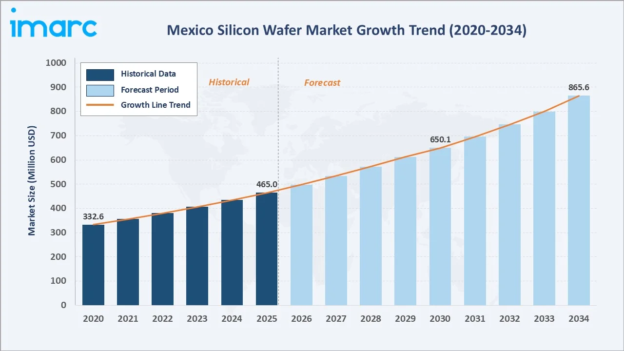
The Mexico silicon wafer market grew from USD 465.0 Million in 2025 to USD 497.2 Million in 2026 and is projected to reach USD 865.6 Million by 2034, growing at a CAGR of 6.93% during 2026-2034. The market is driven by strong demand from automotive electronics, consumer devices, and solar energy applications, supported by Mexico emergence as a nearshoring hub for North American semiconductor supply chains. In February 2025, President Claudia Sheinbaum launched the Kutsari project to strengthen Mexico semiconductor industry, announcing the creation of a National Semiconductor Design Center with facilities in Puebla, Jalisco, and Sonora, driving the growth of the market. P-type leads at 67.5% by type, integrated circuits dominate at 48.6% by application, and Northern Mexico commands the largest regional share at 46.7% in 2025.
Market Snapshot
|
Metric |
Value |
|
Base Year Market Size (2025) |
USD 465.0 Million |
|
Market Size (2026) |
USD 497.2 Million |
|
Forecast Market Size (2034) |
USD 865.6 Million |
|
CAGR (2026-2034) |
6.93% |
|
Base Year |
2025 |
|
Historical Period |
2020-2025 |
|
Forecast Period |
2026-2034 |
|
Dominant Type |
P-type (67.5%, 2025) |
|
Dominant Application |
Integrated Circuits (48.6%, 2025) |
|
Leading Region |
Northern Mexico (46.7%, 2025) |
The Mexico silicon wafer market grew from USD 332.6 Million in 2020 to USD 465.0 Million in 2025, and further to USD 497.2 Million in 2026, reflecting accelerating demand from nearshoring semiconductor operations, automotive electrification, and solar energy expansion. The market is projected to reach USD 650.1 Million by 2030 before reaching USD 865.6 Million by 2034.
To get more information on this market, Request Sample
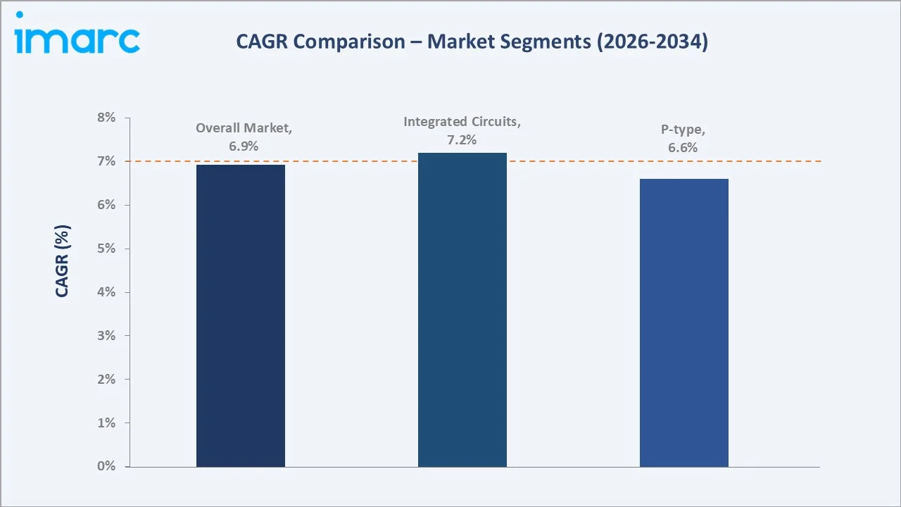
P-type wafers are growing at a 6.6% CAGR, maintaining dominance across established integrated circuit and consumer electronics applications. Integrated circuits at 7.2% CAGR reflect the accelerating semiconductor manufacturing investment in Mexico driven by US CHIPS Act nearshoring. The overall market CAGR of 6.93% reflects Mexico growing strategic importance in the North American semiconductor supply chain and its transition from an assembly and testing hub toward a design and advanced manufacturing ecosystem.
Executive Summary
The Mexico silicon wafer market is on a high-growth trajectory, driven by the convergence of nearshoring semiconductor investments, accelerating automotive electrification generating demand for automotive-grade silicon wafers, rapid solar energy expansion creating high-volume solar cell wafer demand, and the Mexican government's Kutsari program that establishes a formal national semiconductor development strategy.
P-type silicon wafers at 67.5% constitute the dominant wafer type, serving the established integrated circuit fabrication, consumer electronics, and legacy automotive semiconductor applications that represent the majority of current demand. Integrated circuits at 48.6% lead by application, supported by Mexico Jalisco state hosting most of Mexico semiconductor firms. Northern Mexico leads at 46.7%, which has attracted the majority of semiconductor-related foreign investments.
Key Market Insights
|
Insight |
Data |
|
Dominant Type |
P-type - 67.5% share (2025) |
|
Dominant Application |
Integrated Circuits - 48.6% share (2025) |
|
Leading Region |
Northern Mexico - 46.7% (2025) |
|
Key Market Opportunity |
Growing semiconductor manufacturing, increasing investment in domestic chip fabrication, expansion of electronics and automotive industries, and rising demand for advanced semiconductor technologies. |
Key Analytical Observations Supporting the Above Data:
- P-type at 67.5%: P-type silicon wafers dominate because they are the established substrate technology for the majority of commercial semiconductor devices currently manufactured in or for Mexico market, including CMOS logic integrated circuits, microcontrollers, power management ICs, and standard solar cells.
- Integrated Circuits at 48.6%: Integrated circuits lead by application because Mexico semiconductor ecosystem is anchored by IC assembly, testing, and packaging operations serving US fabless semiconductor companies and systems manufacturers.
- Northern Mexico at 46.7%: Northern Mexico leads because the region developed the most advanced semiconductor manufacturing ecosystems in Mexico, benefiting from proximity to the United States, established industrial infrastructure, skilled engineering talent, and facilitated supply chain integration that has attracted the largest concentration of semiconductor-related foreign investment in the country.
Mexico Silicon Wafer Market Overview
The Mexico silicon wafer market encompasses the production, import, distribution, and consumption of all silicon wafer products used in semiconductor device fabrication, solar cell manufacturing, and photonic device production. Silicon wafers serve as the fundamental substrate material on which all semiconductor devices, from simple transistors to complex microprocessors, are fabricated through photolithography, deposition, etching, and doping processes. Mexico silicon wafer market is strategically positioned within the North American semiconductor supply chain, serving both domestic semiconductor manufacturing operations and the growing domestic solar energy market.
Market Dynamics
To evaluate market opportunities, Request Sample
Market Drivers
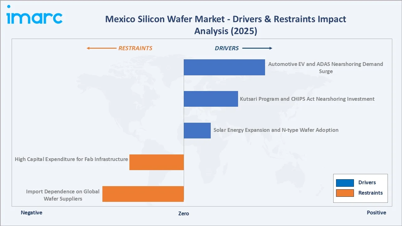
- Automotive EV and ADAS Nearshoring Demand Surge: BEV sales in Mexico reached 37,000 vehicles in 2025, representing an 85% increase from approximately 20,000 units in 2024. Modern vehicles integrate high semiconductor chips per unit for infotainment, ADAS, powertrain, and connectivity functions.
- Kutsari Program and CHIPS Act Nearshoring Investment: In February 2025, President Claudia Sheinbaum launched the Kutsari project to strengthen Mexico semiconductor industry. The initiative created the National Semiconductor Design Center with three facilities in Puebla, Jalisco, and Sonora. These initiatives are attracting investment in semiconductor fabrication, packaging, testing, and supporting supply chains. Growing local production capacity is expected to create additional demand for silicon wafers and other semiconductor-grade materials.
- Solar Energy Expansion and N-type Wafer Adoption: Mexico rapid solar energy deployment, driven by abundant sunlight, falling solar panel costs, and ambitious renewable energy targets, is generating growing demand for solar-grade silicon wafers. N-type wafers are increasingly preferred in high-efficiency solar cell architectures that require N-type substrates. The combination of solar energy expansion and the efficiency premium of N-type solar cells is driving progressive N-type market share gains within the overall silicon wafer market.
Market Restraints
- Import Dependence on Global Wafer Suppliers: Mexico does not produce silicon wafers domestically and relies entirely on imports from global suppliers, primarily sourced from Japan, Germany, Taiwan, and South Korea. This import dependence creates supply chain vulnerability to global semiconductor cycle fluctuations, freight cost variations, and currency exchange dynamics that affect wafer procurement costs for Mexico-based semiconductor manufacturers.
- High Capital Expenditure for Fab Infrastructure: Establishing silicon wafer manufacturing capacity in Mexico would require multi-billion dollar capital investment in crystal growing, wafer slicing, and polishing equipment that currently has no domestic precedent. Even for downstream semiconductor device manufacturing, advanced fabs require more capital investment that represents a barrier to Mexico rapid progression up the semiconductor manufacturing value chain despite the favorable policy environment.
Market Opportunities
- N-type Wafer Premium Market for EV Power Electronics: N-type silicon wafers are increasingly specified for EV power electronics applications, including insulated-gate bipolar transistors (IGBTs) and silicon carbide (SiC) device compatibility, where N-type substrate properties enable higher efficiency power conversion. Mexico growing EV manufacturing sector creates a growing domestic application base for premium N-type wafer consumption.
- Solar Manufacturing Hub Development: Mexico abundant solar resource base and competitive manufacturing cost structure position it as a potential solar panel manufacturing hub serving North American clean energy demand. Establishing solar cell manufacturing in Mexico would create direct silicon wafer demand, and the USMCA supply chain efficiency for solar panel assembly serving US markets provides favorable economics for Mexico-based solar manufacturing investment.
Market Challenges
- Limited Domestic Wafer Manufacturing Capacity: Mexico’s semiconductor ecosystem remains more concentrated in assembly, testing, and packaging than in wafer fabrication. Limited domestic wafer production increases reliance on imported silicon wafers and upstream semiconductor materials.
- Shortage of Specialized Technical Talent: The expansion of semiconductor manufacturing requires engineers and technicians with expertise in wafer processing, semiconductor materials, equipment operation, and quality management. Limited availability of specialized talent can constrain the pace of capacity expansion.
Emerging Market Trends
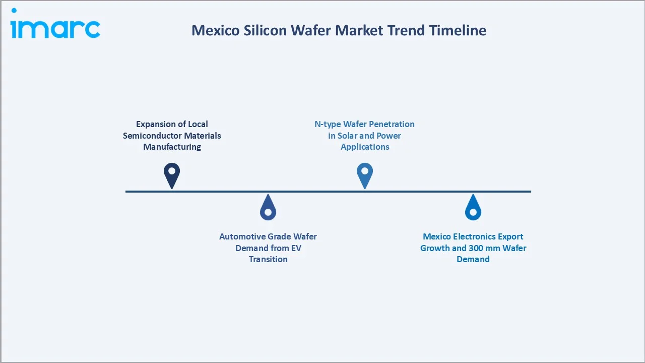
1. Expansion of Local Semiconductor Materials Manufacturing
In August 2026, Indium Corporation opened a new advanced manufacturing facility in Guadalajara, Mexico, strengthening its production and quality capabilities. The facility is expected to support innovation and growing demand across AI, automotive, EVs, robotics, energy storage, and advanced semiconductor packaging. This expansion is supporting regional supply chains and strengthening the country’s capacity to serve high-growth applications such as EVs, AI, energy storage, and advanced semiconductor packaging.
2. Automotive Grade Wafer Demand from EV Transition
Mexico automotive sector electrification is transforming the silicon wafer demand profile from standard consumer-grade wafers toward automotive-qualified wafers with enhanced reliability, traceability, and process control requirements. Automotive silicon wafers must meet quality management requirements and typically command price premiums over standard device wafers.
3. N-type Wafer Penetration in Solar and Power Applications
N-type monocrystalline silicon wafers are growing progressively faster than P-type as solar cell technology upgrades to architectures that require N-type substrates, and as power semiconductor manufacturers shift toward N-type-based IGBTs and MOSFETs for EV and industrial power electronics applications. N-type wafers offer lower oxygen content, longer minority carrier lifetimes, and higher efficiency conversion potential that justify premium pricing in high-performance applications where P-type substrates are no longer technically optimal.
4. Mexico Electronics Export Growth and 300 mm Wafer Demand
In 2024, Mexico exported approximately $113 billion worth of electrical machinery and electronics, ranking as the 9th-largest exporter globally among 226 exporting countries. Mexico electronics exports reflect the rising semiconductor content across automotive and consumer electronics products manufactured domestically. This export growth is progressively pulling semiconductor manufacturing toward larger wafer sizes that enable the economies of scale required for cost-competitive advanced semiconductor production. The transition represents a significant market quality upgrade that increases wafer consumption value even with flat unit volume growth.
Industry Value Chain Analysis
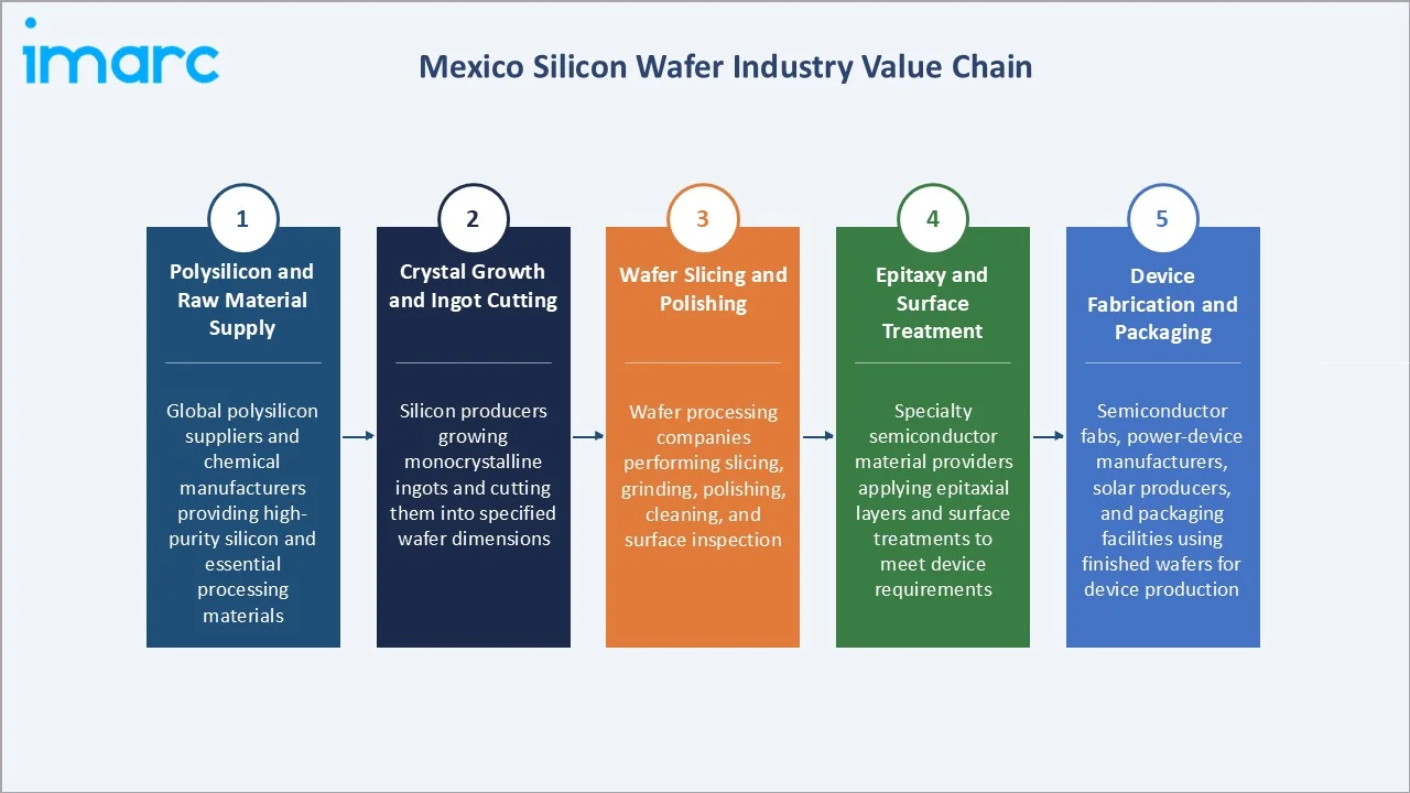
The Mexico silicon wafer market value chain spans five integrated stages from polysilicon raw material supply through device fabrication and packaging. The wafer slicing and polishing stage captures the highest technical value addition in the manufacturing chain, as the precision surface finishing, defect control, and specification compliance that define wafer quality are established at this stage and determine suitability for all downstream semiconductor processes.
|
Stage |
Key Participants |
|
Polysilicon and Raw Material Supply |
Global polysilicon suppliers and chemical manufacturers providing high-purity silicon and essential processing materials. |
|
Crystal Growth and Ingot Cutting |
Silicon producers growing monocrystalline ingots and cutting them into specified wafer dimensions. |
|
Wafer Slicing and Polishing |
Wafer processing companies performing slicing, grinding, polishing, cleaning, and surface inspection. |
|
Epitaxy and Surface Treatment |
Specialty semiconductor material providers applying epitaxial layers and surface treatments to meet device requirements. |
|
Device Fabrication and Packaging |
Semiconductor fabs, power-device manufacturers, solar producers, and packaging facilities using finished wafers for device production. |
The wafer slicing and polishing stage is the highest value-added stage in the silicon wafer value chain. Companies that master the precision surface science of achieving sub-nanometer flatness, controlled resistivity, and minimal crystal defect density across the full wafer surface command the technical differentiation and customer qualification relationships that sustain premium pricing and preferred supplier status with leading semiconductor manufacturers.
Technology Landscape in the Mexico Silicon Wafer Industry
N-type Wafer Technology for High-Efficiency Applications
N-type monocrystalline silicon wafers are enabling next-generation solar cell efficiency through various cell architectures that convert sunlight to electricity more efficiently than standard P-type PERC cells, achieving commercial efficiencies for best-in-class PERC. N-type wafers offer intrinsically lower boron-oxygen complex defects, higher minority carrier lifetimes, and better tolerance for metallic impurities that collectively improve photovoltaic conversion efficiency. For EV power electronics, N-type silicon substrates enable lower forward voltage drop in IGBT devices that directly reduces EV power converter energy losses and extends driving range.
300 mm Large Diameter Wafer Transition
The semiconductor industry transition toward 300 mm wafer manufacturing is progressively defining the quality baseline for competitive semiconductor manufacturing globally. Mexico semiconductor facilities that transition from 200 mm to 300 mm wafer processing gain significant cost-per-chip advantages that improve export competitiveness for semiconductors manufactured in Mexico for US and global markets. This diameter upgrade is supported by continuous improvements in wafer flatness, defect density reduction, and edge exclusion zone minimization by leading wafer suppliers.
Epitaxial Wafer Technology for Automotive Applications
Epitaxial silicon wafers, with customized silicon layers deposited on CZ substrates, enable automotive-grade power semiconductor device performance that cannot be achieved on standard polished wafers. P/P+ and N/N+ epitaxial structures enable low-voltage DMOS and CMOS automotive chip designs with the precise resistivity profiles required for automotive-qualified devices. Mexico growing automotive semiconductor ecosystem is progressively requiring automotive-grade epitaxial wafers that meet reliability qualification standards and supply chain traceability requirements.
Market Segmentation Analysis
The report covers the following segments:
|
Segment Category |
Leading Segment |
Market Share |
Year |
|
Wafer Size |
🔒 |
🔒 |
2025 |
|
Type |
P-type |
67.5% |
2025 |
|
Application |
Integrated Circuits |
48.6% |
2025 |
|
End Use |
🔒 |
🔒 |
2025 |
|
Region |
Northern Mexico |
46.7% |
2025 |

By Type
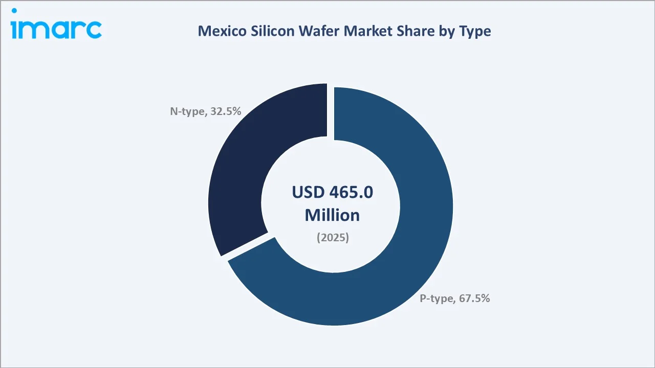
P-type silicon wafers lead at 67.5% in 2025, reflecting the dominance of established semiconductor process flows designed for P-type boron-doped substrates across the majority of Mexico IC assembly, testing, and packaging operations.
To access detailed market analysis, Request Sample
N-type silicon wafers at 32.5% are the fastest-growing type category, gaining market share from superior efficiency in solar cell applications and from power semiconductor device requirements in EV powertrains where N-type IGBTs and MOSFETs offer performance advantages over P-type equivalents.
By Application
Integrated circuits lead at 48.6% in 2025, driven by the IC assembly, testing, and packaging facilities that serve as backend manufacturing nodes for US fabless semiconductor companies.
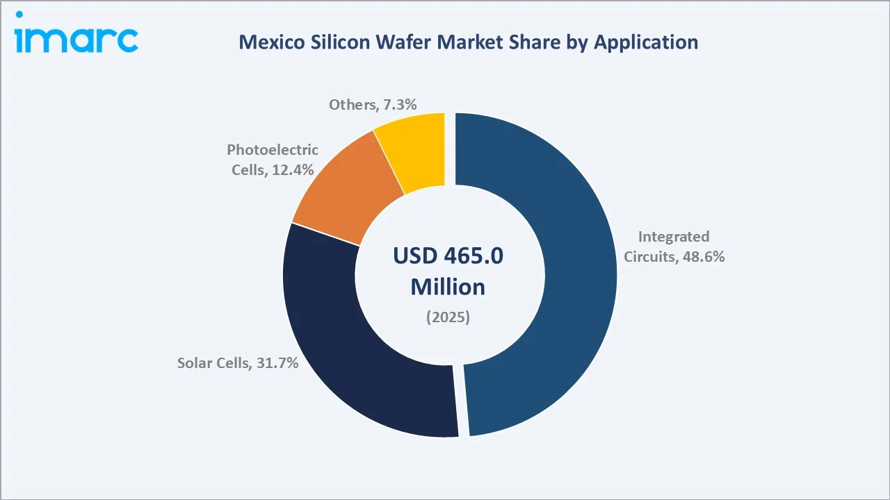
Solar cells at 31.7% represent the second-largest application, reflecting Mexico growing solar energy installation base that is generating demand for solar-grade silicon wafers both for domestic panel manufacturing and as substrate material in solar panels imported for Mexico renewable energy projects. Photoelectric cells at 12.4% cover MEMS sensors, image sensors, and specialty optoelectronic devices. Others at 7.3% include power devices, radio frequency chips, and emerging applications.
Regional Market Insights
|
Region |
Share (2025) |
Key Mexico Silicon Wafer Market Drivers & Characteristics |
|
Northern Mexico |
46.7% |
Strong electronics and automotive manufacturing activities support demand for semiconductor materials and silicon wafers. |
|
Central Mexico |
34.5% |
Growing industrial and electronics clusters are supporting semiconductor-related manufacturing and wafer consumption. |
|
Southern Mexico |
13.8% |
Emerging industrial development and increasing technology investments are gradually supporting market demand. |
|
Others |
5.0% |
Specialized manufacturing activities and developing industrial infrastructure contribute to regional demand. |
Northern Mexico accounted for the largest share of the Mexico silicon wafer market in 2025, representing 46.7%, supported by its strong manufacturing and industrial base. Central Mexico followed with a 34.5% share, driven by expanding electronics and technology-related activities.
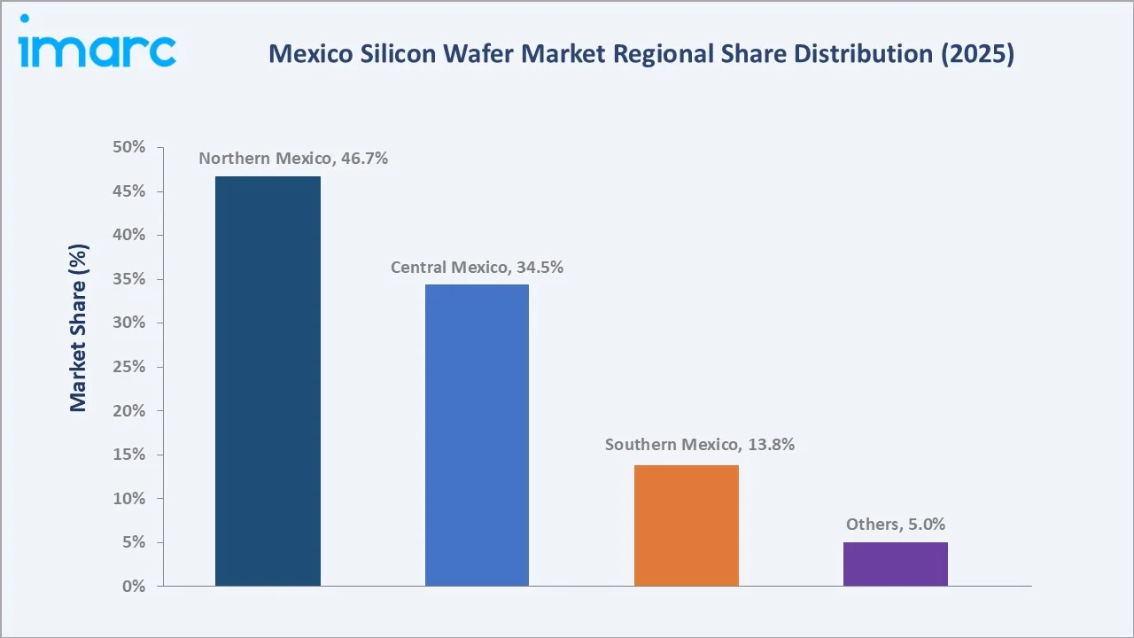
Southern Mexico contributed 13.8%, with emerging industrial development gradually supporting semiconductor-related demand. The other regions held the remaining 5.0% share.
Competitive Landscape
The Mexico silicon wafer market is served entirely by global silicon wafer manufacturers who supply the market through imports, as Mexico does not have domestic silicon wafer production capacity. Competition in the Mexico market is driven by technical wafer specifications, supply reliability, certification for automotive and high-reliability applications, pricing competitiveness on standard volume orders, and responsiveness to Mexico-specific nearshoring demand growth requirements.
| Company | Key Products | Market Position | Core Strength |
|---|---|---|---|
| SUMCO CORPORATION | Epitaxial Wafer (EW), Silicon-On-Insulator (SOI) Wafer | Market Leader | SUMCO Corporation is one of the largest manufacturers of silicon wafers, serving as a foundational supplier for the semiconductor industry. |
| GlobalWafers | Prime Polished Wafer, OPTIA wafer, Perfect Silicon wafers | Market Leader | GlobalWafers is a manufacturer of silicon wafers, supplying the foundational substrate materials used to build virtually all semiconductor chips. |
| Soitec | Silicon-on-Insulator (SOI) wafers | Innovator | Soitec is a leader in designing and manufacturing engineered semiconductor substrates, specifically Silicon-on-Insulator (SOI) wafers. |
| Wafer Works Corp. | Silicon-On-Insulator (SOI) wafers | Challenger | Wafer Works Corp. functions as an established silicon wafer supplier that feeds raw and processed semiconductor substrates into regional supply chains, including the growing market in Mexico. |
The competitive dynamics in Mexico silicon wafer supply are shaped by the global oligopoly structure of the top suppliers, creating limited price competition on premium large-diameter wafers but significant competition on delivery reliability, technical support, and pricing flexibility for standard product orders that serve Mexico semiconductor ATP operations.
Key Company Profiles
SUMCO CORPORATION
SUMCO CORPORATION is a Japan-based manufacturer specializing in high-quality silicon wafers used as substrates for semiconductor devices. The company develops and supplies a range of wafer products for applications across electronics, automotive, industrial, and other semiconductor-related industries. Its operations emphasize advanced wafer technology, quality control, and continuous research and development. SUMCO serves customers globally and supports semiconductor manufacturing through its specialized silicon wafer solutions.
- Key Products: Epitaxial Wafer (EW), Silicon-On-Insulator (SOI) Wafer.
- Strategic Focus: Strengthening its presence in the Mexican semiconductor ecosystem by supporting the growing demand for high-quality silicon wafers. Its strategy emphasizes advanced wafer technologies, consistent product quality, and collaboration with semiconductor manufacturers serving Mexico’s expanding electronics and automotive industries.
GlobalWafers
GlobalWafers is a semiconductor materials company specializing in the production of high-quality silicon wafers and related semiconductor materials. The company serves semiconductor manufacturers across applications including automotive, consumer electronics, communications, and industrial technologies. Its portfolio includes various wafer sizes and specialized products designed to meet diverse semiconductor manufacturing requirements. GlobalWafers maintains a global manufacturing and customer-support network, supporting the semiconductor supply chain in key markets, including Mexico.
- Key Products: Prime Polished Wafer, OPTIA wafer, Perfect Silicon wafers.
- Strategic Focus: Focuses on supporting Mexico’s expanding semiconductor and electronics manufacturing ecosystem through its advanced silicon wafer technologies and global supply capabilities. Its strategy emphasizes strengthening customer relationships, ensuring reliable wafer supply, and supporting growing demand from automotive, electronics, and industrial applications.
Market Concentration Analysis
The Mexico silicon wafer market exhibits very high supply concentration, with the four global wafer leaders, SUMCO CORPORATION, GlobalWafers, Soitec, and Wafer Works Corp., collectively supplying over 90% of global silicon wafer production capacity. This oligopolistic supply structure means that Mexico is entirely dependent on these five companies for silicon wafer procurement, with limited ability to diversify supply through alternative domestic or regional sources. The concentration creates pricing discipline in the global wafer market but also supply chain resilience challenges when capacity constraints emerge. Market concentration at the demand side is moderately high, with Mexico semiconductor activity concentrated that together account for the majority of wafer procurement.
Investment & Growth Opportunities
Highest Growth Segments
Integrated circuits application represents the highest near-term volume growth opportunity, driven by the semiconductor investment announcements expanding Mexico IC assembly, testing, and packaging capacity. N-type wafer supply for solar and EV power electronics represents the highest technology premium growth opportunity, with N-type solar wafers growing significantly faster than the overall market and EV power semiconductor demand commanding automotive-grade pricing premiums.
Investment Themes
- N-type Wafer Supply Chain Development: As Mexico solar cell manufacturing and EV power semiconductor demand grow, establishing reliable N-type wafer supply chains represents a critical procurement infrastructure investment that improves supply security for Mexico technology manufacturers.
- Kutsari Design Center IC Prototyping Wafer Supply: The Kutsari National Semiconductor Design Center creates demand for research-grade and prototype-specification silicon wafers for IC design verification, tape-out, and small-lot fabrication activities that support the transition from design to physical chip production. Establishing wafer supply agreements for this design center prototype wafer segment represents an early-mover opportunity to serve Mexico domestic semiconductor design ecosystem.
Future Market Outlook (2026-2034)
The Mexico silicon wafer market stood at USD 465.0 Million in 2025 and is projected to grow from USD 497.2 Million in 2026 to USD 865.6 Million by 2034, exhibiting a CAGR of 6.93% during the forecast period. The market is expected to reach an intermediate milestone of approximately USD 650.1 Million by 2030, as Kutsari-catalyzed design center activities begin generating domestic prototype wafer demand, and the broader automotive electrification investments translate into automotive-grade silicon wafer consumption at commercial scale.
Three structural forces will define the Mexico silicon wafer market through 2034. First, the nearshoring acceleration driven by the US CHIPS and Science Act will systematically expand Mexico semiconductor manufacturing base beyond its current assembly and testing focus toward higher-value design and potentially front-end fabrication activities, each tier of advancement requiring progressively higher-specification silicon wafers at greater volumes per semiconductor production unit. Second, Mexico automotive sector electrification trajectory will drive structural long-term growth in automotive-grade silicon wafer demand. Third, the Kutsari program represents a formal government commitment that transforms Mexico semiconductor trajectory from a reactive nearshoring host toward a proactive semiconductor ecosystem builder.
Research Methodology
Primary Research
Primary research comprised structured consultations with semiconductor facility managers at Mexico operations, silicon wafer procurement executives at electronics manufacturers, solar energy project developers, automotive tier-1 supplier technical teams, and academic researchers involved in IC design activities. These discussions validated market sizing, assessed nearshoring investment impact on wafer demand, identified technology transition drivers, and provided competitive intelligence on wafer supplier qualification and purchasing dynamics.
Secondary Research
Secondary research drew on IMARC Group market data, Mexico electronics and semiconductor industry export statistics, global silicon wafer market analyses, and company investor relations materials. Historical market data spanning 2020 through 2025 was cross-validated across multiple sources.
Forecasting Models
Market forecasts incorporated nearshoring semiconductor investment pipeline projections, automotive EV production ramp modeling for Mexico, solar energy installation capacity growth forecasts, Kutsari program IC design activity wafer demand projections, N-type versus P-type market share shift modeling, and macroeconomic indicators including Mexico GDP growth and electronics export trajectory through 2034.
Mexico Silicon Wafer Market Report Coverage:
| Report Features | Details |
|---|---|
| Base Year of the Analysis | 2025 |
| Historical Period | 2020-2025 |
| Forecast Period | 2026-2034 |
| Units | Million USD |
| Scope of the Report |
Exploration of Historical Trends and Market Outlook, Industry Catalysts and Challenges, Segment-Wise Historical and Future Market Assessment:
|
| Wafer Sizes Covered | 0–100 mm, 100–200 mm, 200–300 mm, More than 300 mm |
| Types Covered | N-type, P-type |
| Applications Covered | Solar Cells, Integrated Circuits, Photoelectric Cells, Others |
| End Uses Covered | Consumer Electronics, Automotive, Industrial, Telecommunications, Others |
| Regions Covered | Northern Mexico, Central Mexico, Southern Mexico, Others |
| Companies Covered | SUMCO CORPORATION, GlobalWafers, Soitec, Wafer Works Corp., etc. |
| Customization Scope | 10% Free Customization |
| Post-Sale Analyst Support | 10-12 Weeks |
| Delivery Format | PDF and Excel through Email (We can also provide the editable version of the report in PPT/Word format on special request) |
Key Benefits for Stakeholders:
- IMARC’s industry report offers a comprehensive quantitative analysis of various market segments, historical and current market trends, market forecasts, and dynamics of the Mexico silicon wafer market from 2020-2034.
- The research report provides the latest information on the market drivers, challenges, and opportunities in the Mexico silicon wafer market.
- Porter's five forces analysis assist stakeholders in assessing the impact of new entrants, competitive rivalry, supplier power, buyer power, and the threat of substitution. It helps stakeholders to analyze the level of competition within the Mexico silicon wafer industry and its attractiveness.
- Competitive landscape allows stakeholders to understand their competitive environment and provides an insight into the current positions of key players in the market.
Frequently Asked Questions About the Mexico Silicon Wafer Market Report
The Mexico silicon wafer market reached USD 497.2 Million in 2026, driven by automotive electronics nearshoring, solar energy expansion, and the February 2025 Kutsari semiconductor program launch that is accelerating Mexico semiconductor ecosystem development and investment.
The market is projected to grow at a CAGR of 6.93% during 2026-2034, supported by the US CHIPS Act nearshoring driving semiconductor investments in Mexico, automotive EV silicon wafer demand growth, and solar cell expansion.
The market is projected to reach approximately USD 650.1 Million by 2030, as Kutsari National Semiconductor Design Center prototype wafer activities scale, and EV hubs and broader automotive electrification investments generate automotive-grade silicon wafer demand at commercial volume.
P-type leads with a 67.5% share in 2025, reflecting the established process technology dominance of P-type boron-doped silicon wafers in the majority of IC, consumer electronics, and standard power semiconductor applications currently manufactured in or for Mexico semiconductor cluster operations.
Integrated circuits lead with a 48.6% share in 2025, driven by Jalisco state hosting most of Mexico semiconductor firms, which generate the dominant IC-application silicon wafer demand in the country.
Northern Mexico leads with a 46.7% share in 2025, anchored by the semiconductor manufacturing concentration in Jalisco, Chihuahua, Nuevo Leon, and Sonora that together attracted semiconductor-related foreign investment announcements and host the majority of Mexico semiconductor industry activity.
Key players include SUMCO CORPORATION, GlobalWafers, Soitec, and Wafer Works Corp., among others.
The market is projected to reach USD 865.6 Million by 2034, driven by sustained nearshoring semiconductor investment, automotive EV silicon wafer demand from EV manufacturing, solar energy expansion, N-type wafer adoption for high-efficiency applications, and potential progress toward domestic IC fabrication.
Need more help?
- Speak to our experienced analysts for insights on the current market scenarios.
- Include additional segments and countries to customize the report as per your requirement.
- Gain an unparalleled competitive advantage in your domain by understanding how to utilize the report and positively impacting your operations and revenue.
- For further assistance, please connect with our analysts.
 Request Customization
 Speak to an Analyst
 Request Brochure
 Inquire Before Buying
Benefits of Customization
- Personalize this research
- Triangulate with your data
- Get data as per your format and definition
- Gain a deeper dive into a specific application, geography, customer, or competitor
- Any level of personalization
Get in Touch With Us
UNITED STATES
Phone: +1-201-971-6302
INDIA
Phone: +91-120-433-0800
UNITED KINGDOM
Phone: +44-753-714-6104
Email: [email protected]
Client Testimonials




.webp)



.webp)











Related Reports

Choose your plan
*Please note that the prices mentioned below are starting prices for each bundle type. Kindly contact our team for further details.*
Single User License
- 1 User License, Access on 2 Devices
- PDF Report + Excel Dataset (Password Protected)
- Lifetime Access
- No Printing Rights
- 10% Free Report Customization
- 10–12 Weeks of Analyst Support
Five User License
- Access for 5 Users, 2 Devices per User
- PDF Report + Excel Dataset (Password Protected)
- Lifetime Access
- Dedicated Account Manager
- 12–14 Weeks of Analyst Support
- No Printing Rights
- 15% Free Report Customization
- 25% Discount on Your Next Purchase
Corporate User License
- Unlimited User Access (Within Your Organization)
- PDF Report + Excel Dataset
- Lifetime Access
- Dedicated Account Manager
- 14–20 Weeks of Analyst Support
- No Printing Rights
- 20% Free Report Customization
- 30% Discount on Your Next Purchase
Essential Insights
What's included:
3 reports
- Lifetime Access
- PDF Reports
- Excel Datasets
- 2 Weeks of Free Analyst Support
- 2 User Licenses
- Access on 2 Devices
- Printing Rights
- Complimentary PowerPoint (PPT) Version
- Complimentary License Upgrade
Professional Access
What's included:
5 reports
- Lifetime Access
- PDF Reports
- Excel Datasets
- 8 Weeks of Free Analyst Support
- 2 User Licenses
- Access on 2 Devices
- Printing Rights
- Complimentary PowerPoint (PPT) Version
- Complimentary License Upgrade
Business Advantage
What's included:
8 reports
- Lifetime Access
- PDF Reports
- Excel Datasets
- 14 Weeks of Free Analyst Support
- 2 User Licenses
- Access on 2 Devices
- Printing Rights
- Complimentary PowerPoint (PPT) Version
- Complimentary License Upgrade
Enterprise Intelligence
What's included:
10 reports
- Lifetime Access
- PDF Reports
- Excel Datasets
- 20 Weeks of Free Analyst Support
- 2 User Licenses
- Access on 2 Devices
- Printing Rights
- Complimentary PowerPoint (PPT) Version
- Complimentary License Upgrade