Patterning Material Market Report by Type (I-line and g-line, Positive 248 nm, Positive 193 nm Dry Resist, Positive 193 nm Immersion Resist, and Others), Application (Integrated Circuits and PCBs, MEMS and NEMS Devices, Sensors, Dynamic Random Access Memory, and Others), and Region 2026-2034
Market Overview:
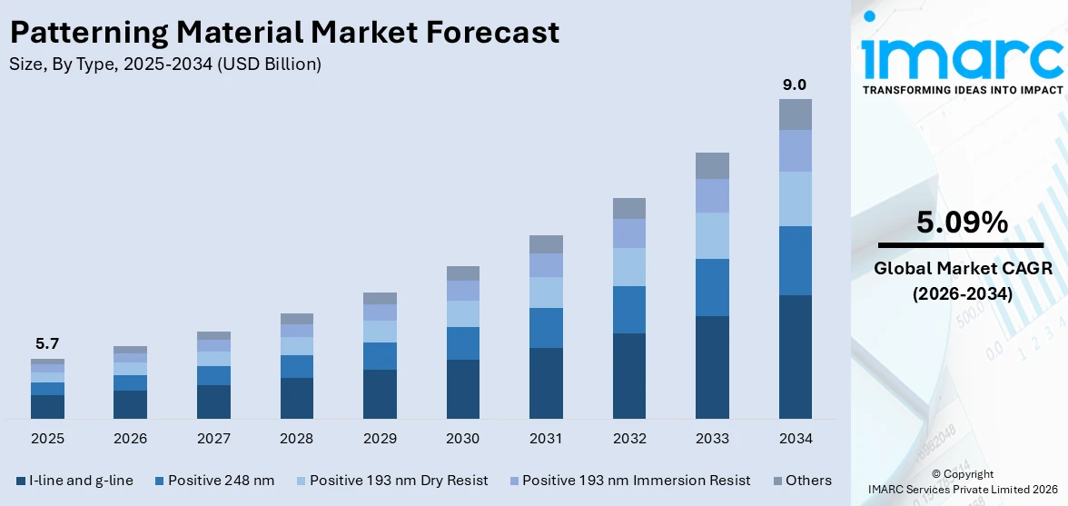
The global patterning material market size reached USD 5.7 Billion in 2025. Looking forward, IMARC Group expects the market to reach USD 9.0 Billion by 2034, exhibiting a growth rate (CAGR) of 5.09% during 2026-2034. The increasing electronics production, the rising semiconductor innovations, the evolving display technologies, and the growing compliance with eco-friendly regulations are some of the factors propelling the market.
|
Report Attribute
|
Key Statistics |
|---|---|
|
Base Year
|
2025 |
|
Forecast Years
|
2026-2034
|
|
Historical Years
|
2020-2025
|
| Market Size in 2025 | USD 5.7 Billion |
| Market Forecast in 2034 | USD 9.0 Billion |
| Market Growth Rate (2026-2034) | 5.09% |
A patterning material, commonly used in manufacturing electronics and semiconductors, is a substance that aids in creating intricate patterns on substrates. It serves as a template for transferring patterns during various fabrication processes. These materials are crucial for lithography, a key step in chip fabrication, where they help define the arrangement of components at a nanoscale level. Photoresists, a type of patterning material, are light-sensitive polymers that undergo chemical changes when exposed to light, allowing for precise pattern transfer onto semiconductor wafers. These materials enable the production of smaller and more powerful electronic devices by defining the features of circuits and structures. Developing new materials is crucial to achieving higher miniaturization and performance in modern electronic products as technology advances.
To get more information on this market Request Sample
The global market is majorly driven by the increasing need for smaller and more powerful electronic devices. In line with this, the expanding electronics industry is significantly contributing to the demand for these materials in semiconductor manufacturing. Furthermore, these materials are crucial for advanced packaging technologies, positively influencing the market. Apart from this, the rising adoption of 5G technology requires precise patterning for high-frequency components, catalyzing the market. Moreover, the growing Internet of Things (IoT) devices require miniaturized components, propelling product demand. Besides, the escalating AI applications necessitate higher computing power, stimulating demand for advanced semiconductors and patterning materials. Additionally, the increasing complexity of automotive electronics and the rising demand for smaller, lighter, and more efficient consumer gadgets are fueling the market.
Patterning Material Market Trends/Drivers:
Increasing product demand in miniaturized medical devices
The increasing demand for miniaturized medical devices is bolstering the market. As medical technology advances, there is a growing emphasis on developing compact yet highly functional medical devices for various applications. These materials play a crucial role in the fabrication of these devices, enabling the creation of intricate and precise structures necessary for their operation. Miniaturized medical devices, such as implantable sensors, medical wearables, and diagnostic tools, require intricate circuitry and components that can be seamlessly integrated into the human body or worn comfortably. Patterning materials, like photoresists, enable the manufacturing of these devices by allowing for precise pattern transfer onto small substrates, ensuring the functionality and reliability of the end product. The demand for such devices is driven by the need for improved patient care, remote monitoring capabilities, and advancements in personalized medicine, all of which contribute to the continued market growth within the medical sector.
Rising investments in research and development activities
The rising research and development (R&D) investments significantly impact the market. Companies, institutions, and governments are allocating substantial resources to innovate and enhance the capabilities of patterning materials. These investments fuel the development of novel materials, advanced manufacturing processes, and cutting-edge technologies that push the boundaries of precision and efficiency in various industries. R&D efforts are focused on improving patterning techniques, enabling finer feature sizes, and reducing manufacturing defects. As industries like electronics, semiconductors, photonics, and more demand higher performance and miniaturization, R&D investments directly contribute to meeting these evolving needs. Additionally, pursuing eco-friendly and sustainable solutions aligns with global trends, further shaping the direction of patterning material research. These investments drive technological advancements and foster collaboration among academia, industry, and research organizations. As a result, the market witnesses accelerated growth, with innovation becoming a driving force behind the continued evolution of materials and processes that underpin modern manufacturing and technology.
Rapid advancements in nanotechnology
Rapid advancements in nanotechnology are offering numerous opportunities for the market. Nanotechnology deals with manipulating materials and structures at the nanoscale, enabling the creation of incredibly small and precise components. These materials play a critical role in this field by facilitating nanoscale patterns and structure fabrication. As researchers explore the potential of nanotechnology across various industries, including electronics, medicine, energy, and materials science, the demand for advanced materials intensifies. These materials enable the creation of intricate nanostructures that form the basis of nanodevices and systems. The ability to accurately pattern materials at such small scales unlocks new opportunities for developing high-performance devices, sensors, catalysts, and more. Rapid advancements in nanotechnology lead to a virtuous cycle, driving the need for more precise and sophisticated materials while benefiting from the capabilities these materials enable. This synergy fosters innovation, expands applications, and propels the market forward as a fundamental enabler of nanotechnology's transformative potential.
Patterning Material Industry Segmentation:
IMARC Group provides an analysis of the key trends in each segment of the global patterning material market report, along with forecasts at the global, regional and country levels for 2026-2034. Our report has categorized the market based on type and application.
Breakup by Type:
- I-line and g-line
- Positive 248 nm
- Positive 193 nm Dry Resist
- Positive 193 nm Immersion Resist
- Others
The report has provided a detailed breakup and analysis of the market based on the type. This includes I-line and g-line, positive 248 nm, positive 193 nm dry resist, positive 193 nm immersion resist, and others.
I-line and g-line materials offer cost-effective solutions for various semiconductor and electronics manufacturing processes, appealing to multiple industries. These materials enable efficient lithography processes, facilitating the creation of intricate patterns on substrates.
The Positive 248 nm segment, specifically, addresses the demand for higher resolution and precision in patterning. As technology trends demand smaller feature sizes, Positive 248 nm materials excel in producing finer patterns, supporting the miniaturization requirements of modern electronics. Their ability to achieve high-resolution patterns makes them indispensable in advanced semiconductor manufacturing and other industries that rely on precise patterning techniques.
Breakup by Application:
Access the comprehensive market breakdown Request Sample
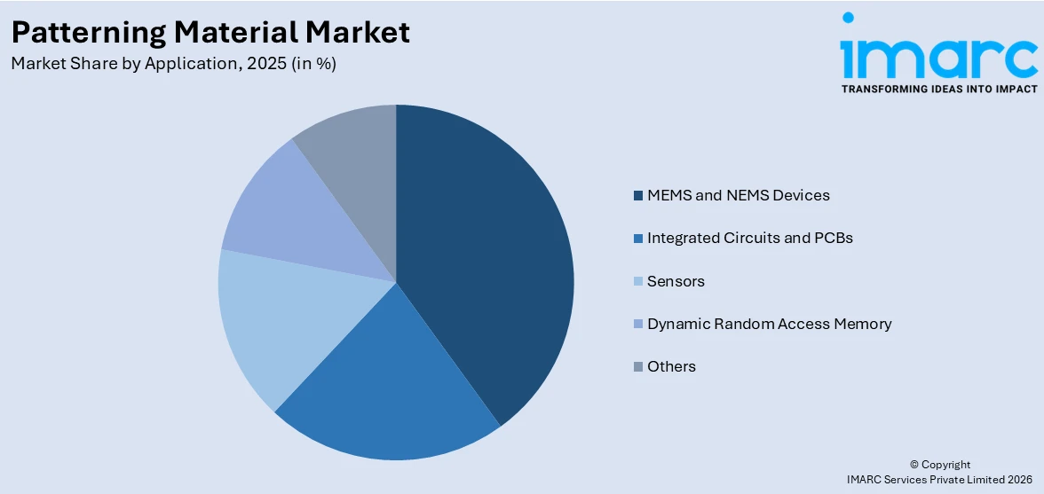
- Integrated Circuits and PCBs
- MEMS and NEMS Devices
- Sensors
- Dynamic Random Access Memory
- Others
MEMS and NEMS devices dominates the market
The report has provided a detailed breakup and analysis of the market based on the application. This includes integrated circuits and PCBs, MEMS and NEMS devices, sensors, dynamic random access memory, and others. According to the report, MEMS and NEMS devices represented the largest segment.
Patterning materials tailored for Integrated Circuits and PCBs manufacturing ensure precise circuitry, facilitating the production of advanced microchips and electronics. These materials enable higher integration and performance in electronic devices, meeting the demand for enhanced computing power and connectivity.
In the MEMS and NEMS devices category, patterning materials are critical in producing miniature mechanical and nanoelectromechanical systems. As these devices become integral to various industries, including automotive, healthcare, and consumer electronics, the demand for specialized patterning materials rises. These materials enable the creation of intricate and functional structures, contributing to the miniaturization and efficiency of MEMS and NEMS devices.
Breakup by Region:
- North America
- United States
- Canada
- Europe
- Germany
- France
- United Kingdom
- Italy
- Spain
- Others
- Asia Pacific
- China
- Japan
- India
- South Korea
- Australia
- Indonesia
- Others
- Latin America
- Brazil
- Mexico
- Others
- Middle East and Africa
Asia Pacific exhibits a clear dominance, accounting for the largest market share
The report has also provided a comprehensive analysis of all the major regional markets, which include North America (the United States and Canada); Europe (Germany, France, the United Kingdom, Italy, Spain, and others); Asia Pacific (China, Japan, India, South Korea, Australia, Indonesia, and others); Latin America (Brazil, Mexico, and others); and the Middle East and Africa. According to the report, Asia Pacific accounted for the largest market share.
As a technology hub, Asia Pacific boasts a robust demand for advanced patterning materials driven by its vibrant electronics, semiconductor, and research industries. The region's continuous innovation and adoption of new technologies fuel the need for precise patterning materials, propelling market expansion.
In Europe, renowned for its manufacturing prowess and strong research collaborations, the demand for advanced patterning materials is driven by various industries, including automotive, aerospace, and telecommunications. The region's emphasis on sustainability further fuels the development of eco-friendly patterning materials, aligning with its environmental goals and influencing the market growth.
Competitive Landscape:
Top companies are fostering the market through strategic initiatives and innovations. These companies invest heavily in research and development, continuously improving patterning materials' performance, reliability, and eco-friendliness. They collaborate closely with semiconductor manufacturers, electronics firms, and various industries to tailor materials to specific application needs. Furthermore, these companies actively partner with research institutions and universities to explore new frontiers in patterning technology. They leverage their expertise to provide comprehensive solutions, offering clients consulting, training, and technical support. With a keen focus on sustainability, these companies drive the development of eco-friendly patterning materials, aligning with industry and regulatory trends. Through technological advancements, customer-centric solutions, and strategic collaborations, top companies stimulate market growth by meeting evolving demands across industries and pushing the boundaries of what is achievable in modern manufacturing and technology.
The report has provided a comprehensive analysis of the competitive landscape in the patterning material market. Detailed profiles of all major companies have also been provided.
- Brewer Science, Inc.
- Dongjin Semichem Co., Ltd
- DuPont de Nemours, Inc.
- Fujifilm Holding Corporation
- Honeywell International Inc.
- JSR Micro, Inc. (JSR Corporation)
- Merck KGaA
- Shin-Etsu Chemical Co., Ltd.
- Sumitomo Chemicals Co, Ltd.
- Tokyo Ohka Kogyo Co., Ltd
Patterning Material Market Report Scope:
| Report Features | Details |
|---|---|
| Base Year of the Analysis | 2025 |
| Historical Period | 2020-2025 |
| Forecast Period | 2026-2034 |
| Units | Billion USD |
| Scope of the Report | Exploration of Historical and Forecast Trends, Industry Catalysts and Challenges, Segment-Wise Historical and Predictive Market Assessment:
|
| Types Covered | I-line and g-line, Positive 248 nm, Positive 193 nm Dry Resist, Positive 193 nm Immersion Resist, Others |
| Applications Covered | Integrated Circuits and PCBs, MEMS and NEMS Devices, Sensors, Dynamic Random Access Memory, Others |
| Regions Covered | Asia Pacific, Europe, North America, Latin America, Middle East and Africa |
| Countries Covered | United States, Canada, Germany, France, United Kingdom, Italy, Spain, China, Japan, India, South Korea, Australia, Indonesia, Brazil, Mexico |
| Companies Covered | Brewer Science, Inc., Dongjin Semichem Co., Ltd, DuPont de Nemours, Inc., Fujifilm Holding Corporation, Honeywell International Inc., JSR Micro, Inc. (JSR Corporation), Merck KGaA, Shin-Etsu Chemical Co., Ltd., Sumitomo Chemicals Co, Ltd., Tokyo Ohka Kogyo Co., Ltd, etc. |
| Customization Scope | 10% Free Customization |
| Post-Sale Analyst Support | 10-12 Weeks |
| Delivery Format | PDF and Excel through Email (We can also provide the editable version of the report in PPT/Word format on special request) |
Key Questions Answered in This Report:
- How has the global patterning material market performed so far, and how will it perform in the coming years?
- What are the drivers, restraints, and opportunities in the global patterning material market?
- What is the impact of each driver, restraint, and opportunity on the global patterning material market?
- What are the key regional markets?
- Which countries represent the most attractive patterning material market?
- What is the breakup of the market based on the type?
- Which is the most attractive type in the global patterning material market?
- What is the breakup of the market based on the application?
- Which is the most attractive application in the global patterning material market?
- What is the competitive structure of the global patterning material market?
- Who are the key players/companies in the global patterning material market?
Key Benefits for Stakeholders:
- IMARC’s report offers a comprehensive quantitative analysis of various market segments, historical and current market trends, market forecasts, and dynamics of the patterning material market from 2020-2034.
- The research study provides the latest information on the market drivers, challenges, and opportunities in the global patterning material market.
- The study maps the leading, as well as the fastest-growing, regional markets. It further enables stakeholders to identify the key country-level markets within each region.
- Porter's five forces analysis assists stakeholders in assessing the impact of new entrants, competitive rivalry, supplier power, buyer power, and the threat of substitution. It helps stakeholders to analyze the level of competition within the patterning material industry and its attractiveness.
- Competitive landscape allows stakeholders to understand their competitive environment and provides an insight into the current positions of key players in the market.
Need more help?
- Speak to our experienced analysts for insights on the current market scenarios.
- Include additional segments and countries to customize the report as per your requirement.
- Gain an unparalleled competitive advantage in your domain by understanding how to utilize the report and positively impacting your operations and revenue.
- For further assistance, please connect with our analysts.
 Request Customization
 Speak to an Analyst
 Request Brochure
 Inquire Before Buying
Benefits of Customization
- Personalize this research
- Triangulate with your data
- Get data as per your format and definition
- Gain a deeper dive into a specific application, geography, customer, or competitor
- Any level of personalization
Get in Touch With Us
UNITED STATES
Phone: +1-201-971-6302
INDIA
Phone: +91-120-433-0800
UNITED KINGDOM
Phone: +44-753-714-6104
Email: [email protected]
Client Testimonials

.webp)