Saudi Arabia Semiconductor Packaging Market Size, Share, Trends and Forecast by Type, Packaging Material, Technology, End User, and Region, 2026-2034
Saudi Arabia Semiconductor Packaging Market Overview:
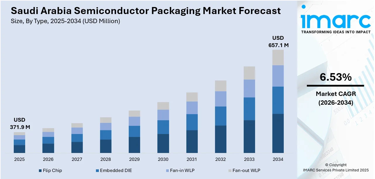
The Saudi Arabia semiconductor packaging market size reached USD 371.9 Million in 2025. Looking forward, IMARC Group expects the market to reach USD 657.1 Million by 2034, exhibiting a growth rate (CAGR) of 6.53% during 2026-2034. Saudi Arabia’s market is expanding due to rising government investment, talent development programs, and growing interest from global chipmakers. Initiatives under the National Semiconductor Hub are accelerating local design, assembly, and packaging capabilities, supporting Vision 2030’s push for advanced technology self-reliance.
|
Report Attribute
|
Key Statistics
|
|---|---|
|
Base Year
|
2025
|
|
Forecast Years
|
2026-2034
|
|
Historical Years
|
2020-2025
|
| Market Size in 2025 | USD 371.9 Million |
| Market Forecast in 2034 | USD 657.1 Million |
| Market Growth Rate 2026-2034 | 6.53% |
Saudi Arabia Semiconductor Packaging Market Trends:
Increased Government Funding and Incentives
Saudi Arabia’s semiconductor packaging market has gained strong forward momentum through focused government backing, primarily via large-scale financial incentives and strategic national initiatives. This policy shift is attracting international chipmakers and helping to establish a homegrown ecosystem for chip packaging and related services. The National Semiconductor Hub (NSH) is central to this movement, supporting companies through funding, infrastructure, and talent development. In June 2024, the government unveiled a USD 266.5 Million tech fund as part of this strategy. The fund, created with backing from deep-tech venture capital firms, is intended to support the formation of a USD 13.33 Billion domestic semiconductor industry over six years. The initiative includes a 10-point incentive plan offering operational capital, premium residency programs, and workforce relocation packages to chipmakers. Saudi Arabia also plans to onboard 25 international experts and train 5,000 engineers to drive the local industry. These developments directly support the growth of the semiconductor packaging segment by creating conditions that reduce entry barriers and improve scalability. The incentives help attract companies focused on integrated circuit design, packaging, and final testing stages, all essential parts of the value chain. Through consistent capital injection and structured support mechanisms, Saudi Arabia is laying a foundation for sustainable growth in advanced chip packaging operations.
To get more information on this market Request Sample
Strengthening Local Design and Fabrication Capabilities
A parallel driver of growth in Saudi Arabia’s semiconductor packaging market is the deliberate push to build and enhance local capabilities in chip design, fabrication, and assembly. Rather than only serving as a destination for foreign companies, the Kingdom is setting the stage for domestic engineering excellence, which plays a direct role in downstream packaging growth. The National Semiconductor Hub has played a key role by enabling partnerships, offering development grants, and ensuring access to critical manufacturing infrastructure. In February 2025, NSH announced its plan for Saudi Arabia’s first chip tapeout, scheduled for July, marking a major milestone in local fabrication efforts. This initiative reflects a shift from dependency on imported components to creating value through internal design and production resources. The presence of fabless companies working on AI chips and specialized processors within the NSH ecosystem ensures a continuous demand for advanced semiconductor packaging services locally. With more companies establishing design teams and technical offices in Riyadh, demand for high-performance, efficient, and scalable packaging solutions is expected to grow. The development is not limited to front-end design but extends into back-end services, including assembly and testing. By enabling domestic chip production, Saudi Arabia is ensuring its packaging market matures in parallel with design and fabrication, driving end-to-end industry capability.
Saudi Arabia Semiconductor Packaging Market Segmentation:
IMARC Group provides an analysis of the key trends in each segment of the market, along with forecasts at the region/country level for 2026-2034. Our report has categorized the market based on type, packaging material, technology, and end user.
Type Insights:
- Flip Chip
- Embedded DIE
- Fan-in WLP
- Fan-out WLP
The report has provided a detailed breakup and analysis of the market based on the type. This includes flip chip, embedded DIE, fan-in WLP, and fan-out WLP.
Packaging Material Insights:
- Organic Substrate
- Bonding Wire
- Leadframe
- Ceramic Package
- Die Attach Material
- Others
A detailed breakup and analysis of the market based on the packaging material have also been provided in the report. This includes organic substrate, bonding wire, leadframe, ceramic package, die attach material, and others.
Technology Insights:
- Grid Array
- Small Outline Package
- Flat no-leads Package
- Dual In-Line Package
- Others
A detailed breakup and analysis of the market based on the technology have also been provided in the report. This includes grid array, small outline package, flat no-leads package, dual in-line package, and others.
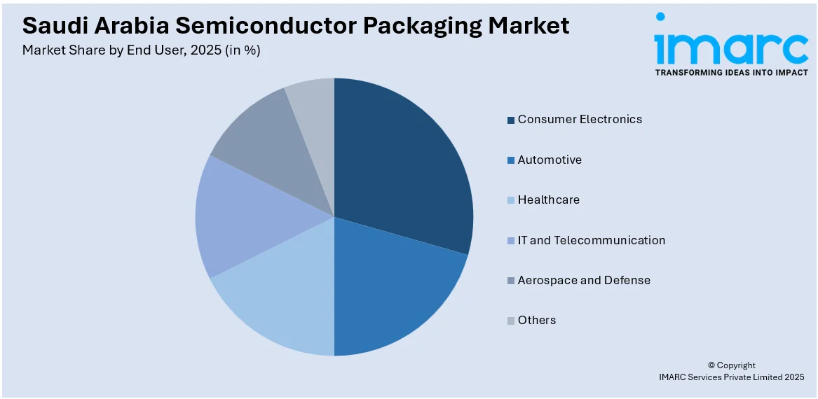
End User Insights:
Access the comprehensive market breakdown Request Sample
- Consumer Electronics
- Automotive
- Healthcare
- IT and Telecommunication
- Aerospace and Defense
- Others
A detailed breakup and analysis of the market based on the end user have also been provided in the report. This includes consumer electronics, automotive, healthcare, it and telecommunication, aerospace and defense, and others.
Regional Insights:
- Northern and Central Region
- Western Region
- Eastern Region
- Southern Region
The report has also provided a comprehensive analysis of all the major regional markets, which include Northern and Central region, Western region, Eastern region, and Southern region.
Competitive Landscape:
The market research report has also provided a comprehensive analysis of the competitive landscape. Competitive analysis such as market structure, key player positioning, top winning strategies, competitive dashboard, and company evaluation quadrant has been covered in the report. Also, detailed profiles of all major companies have been provided.
Saudi Arabia Semiconductor Packaging Market News:
- February 2025: EdgeCortix established a subsidiary in Saudi Arabia after being selected for the National Semiconductor Hub. This move supported advanced chip engineering and edge AI development, boosting local semiconductor packaging capabilities, attracting investments, and accelerating Vision 2030-driven tech ecosystem growth in the Kingdom.
- January 2025: Kneron launched a subsidiary in Riyadh through Saudi Arabia’s National Semiconductor Hub. The move supported local semiconductor packaging by advancing AI chip development, promoting technology transfer, and fostering talent, strengthening the Kingdom’s semiconductor ecosystem under Vision 2030 goals.
Saudi Arabia Semiconductor Packaging Market Report Coverage:
| Report Features | Details |
|---|---|
| Base Year of the Analysis | 2025 |
| Historical Period | 2020-2025 |
| Forecast Period | 2026-2034 |
| Units | Million USD |
| Scope of the Report |
Exploration of Historical Trends and Market Outlook, Industry Catalysts and Challenges, Segment-Wise Historical and Future Market Assessment:
|
| Types Covered | Flip Chip, Embedded DIE, Fan-in WLP, Fan-out WLP |
| Packaging Materials Covered | Organic Substrate, Bonding Wire, Leadframe, Ceramic Package, Die Attach Material, Others |
| Technologies Covered | Grid Array, Small Outline Package, Flat no-leads Package, Dual In-Line Package, Others |
| End Uses Covered | Consumer Electronics, Automotive, Healthcare, IT and Telecommunication, Aerospace and Defense, Others |
| Regions Covered | Northern and Central Region, Western Region, Eastern Region, Southern Region |
| Customization Scope | 10% Free Customization |
| Post-Sale Analyst Support | 10-12 Weeks |
| Delivery Format | PDF and Excel through Email (We can also provide the editable version of the report in PPT/Word format on special request) |
Key Questions Answered in This Report:
- How has the Saudi Arabia semiconductor packaging market performed so far and how will it perform in the coming years?
- What is the breakup of the Saudi Arabia semiconductor packaging market on the basis of the type?
- What is the breakup of the Saudi Arabia semiconductor packaging market on the basis of packaging material?
- What is the breakup of the Saudi Arabia semiconductor packaging market on the basis of technology?
- What is the breakup of the Saudi Arabia semiconductor packaging market on the basis of end user?
- What are the various stages in the value chain of the Saudi Arabia semiconductor packaging market?
- What are the key driving factors and challenges in the Saudi Arabia semiconductor packaging?
- What is the structure of the Saudi Arabia semiconductor packaging market and who are the key players?
- What is the degree of competition in the Saudi Arabia semiconductor packaging market?
Key Benefits for Stakeholders:
- IMARC’s industry report offers a comprehensive quantitative analysis of various market segments, historical and current market trends, market forecasts, and dynamics of the Saudi Arabia semiconductor packaging market from 2020-2034.
- The research report provides the latest information on the market drivers, challenges, and opportunities in the Saudi Arabia semiconductor packaging market.
- Porter's five forces analysis assist stakeholders in assessing the impact of new entrants, competitive rivalry, supplier power, buyer power, and the threat of substitution. It helps stakeholders to analyze the level of competition within the Saudi Arabia semiconductor packaging industry and its attractiveness.
- Competitive landscape allows stakeholders to understand their competitive environment and provides an insight into the current positions of key players in the market.
Need more help?
- Speak to our experienced analysts for insights on the current market scenarios.
- Include additional segments and countries to customize the report as per your requirement.
- Gain an unparalleled competitive advantage in your domain by understanding how to utilize the report and positively impacting your operations and revenue.
- For further assistance, please connect with our analysts.
 Request Customization
 Speak to an Analyst
 Request Brochure
 Inquire Before Buying
Benefits of Customization
- Personalize this research
- Triangulate with your data
- Get data as per your format and definition
- Gain a deeper dive into a specific application, geography, customer, or competitor
- Any level of personalization
Get in Touch With Us
UNITED STATES
Phone: +1-201-971-6302
INDIA
Phone: +91-120-433-0800
UNITED KINGDOM
Phone: +44-753-714-6104
Email: [email protected]
Client Testimonials
.webp)