United States Photoresist and Photoresist Ancillaries Market Report by Photoresist Type (ArF Immersion, KrF, ArF Dry, g- and i-line), Photoresist Ancillaries Type (Anti-Reflective Coatings, Remover, Developer, and Others), Application (Semiconductors & ICS, LCDs, Printed Circuit Boards, and Others), and Region 2026-2034
Market Overview:
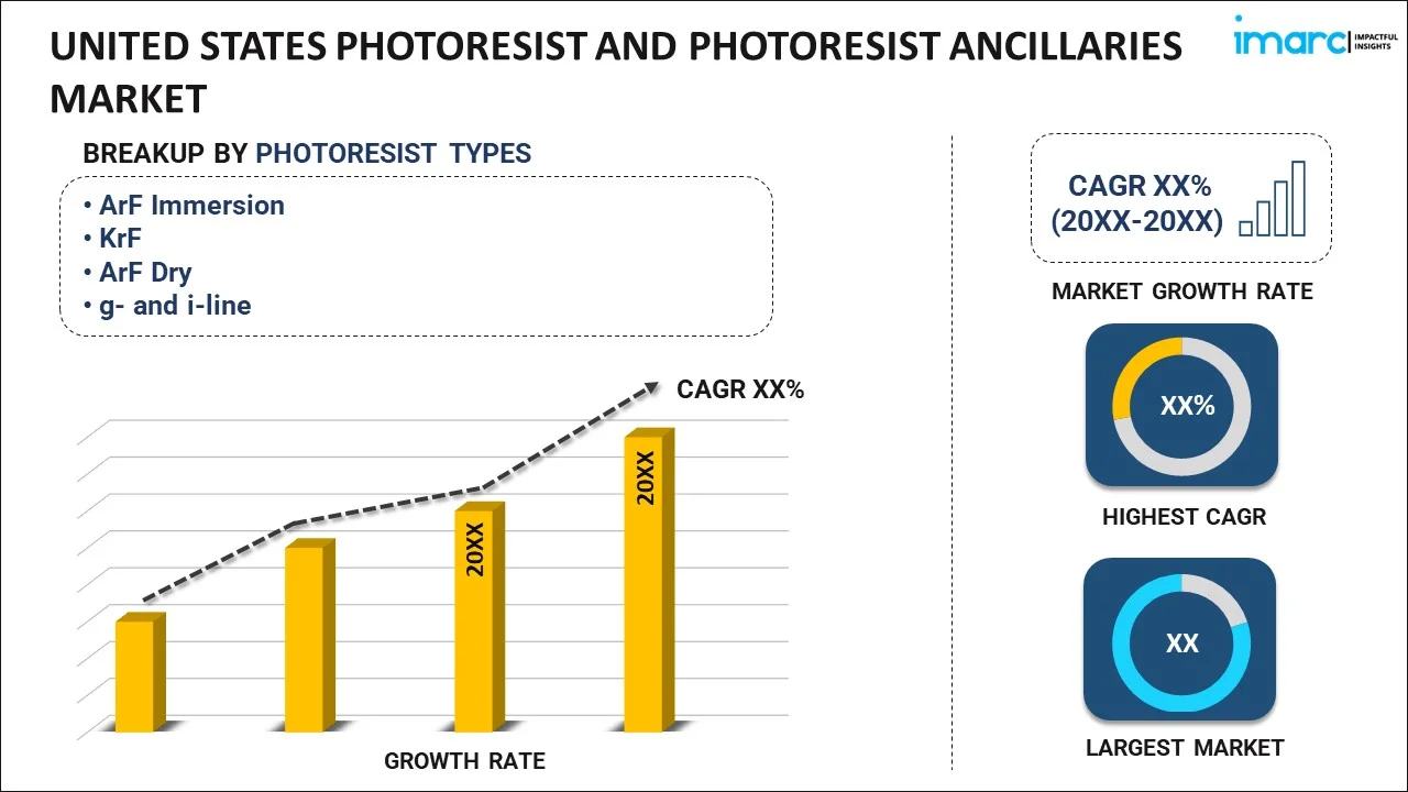
The United States photoresist and photoresist ancillaries market size reached USD 1,044.6 Million in 2025. Looking forward, IMARC Group expects the market to reach USD 1,523.4 Million by 2034, exhibiting a growth rate (CAGR) of 4.28% during 2026-2034.
|
Report Attribute
|
Key Statistics
|
|---|---|
|
Base Year
|
2025 |
|
Forecast Years
|
2026-2034
|
|
Historical Years
|
2020-2025
|
| Market Size in 2025 | USD 1,044.6 Million |
| Market Forecast in 2034 | USD 1,523.4 Million |
| Market Growth Rate (2026-2034) | 4.28% |
Access the full market insights report Request Sample
United States Photoresist and Photoresist Ancillaries Market Analysis:
- Major Drivers: Expansion of domestic semiconductor manufacturing, government policy support, and rising demand for electronics in automotive, artificial intelligence (AI), and fifth generation (5G) sectors are driving the need for advanced photoresists and ancillary materials.
- Key Market Trends: Growing adoption of advanced lithography techniques, increased demand for high-resolution semiconductors, and rising focus on green photoresist formulations are shaping product development and influencing material selection across the semiconductor ecosystem thus bolstering the United States photoresist and photoresist ancillaries market growth.
- Market Opportunities: Development of EUV-compatible resists, environmentally friendly chemistries, and localized supply chains present opportunities. Collaborations between chipmakers and chemical producers can drive innovation and secure long-term technological and commercial advantages.
- Market Challenges: Complex manufacturing processes, extreme research and development (R&D) investments, skilled labor shortages, and geopolitical concerns affecting global supply chains create obstacles to scaling production and maintaining competitiveness in this highly specialized materials market are some of the factors impeding the market demand in the United States photoresist and photoresist ancillaries market analysis.
A photoresist is a photosensitive material that can change its chemical structure when exposed to ultraviolet light. Photoresist ancillaries are supporting products that are used to improve the efficiency and resolution of the photolithography or photoengraving process. Resins with the desired solvent and a photo active generator (PAG) compound are the basic raw materials used to manufacture photoresist chemicals and ancillaries. Positive photoresists are soluble, while negative photoresists become insoluble and cross-linked when exposed to UV light. They are used in flat panel displays and wiring configurations for the manufacturing of multi-layer semiconductors.
The United States photoresist and photoresist ancillaries market is primarily driven by the flourishing semiconductor industry. The trend of miniaturization in the semiconductor industry has enabled the development of advanced technologies that now form the backbone of the modern electronics industry. This has been supported by the development of polymer-based photoresist materials and consequent advances in the photolithography process. These advances have led to the evolution of microfabrication technology resulting in higher-level integration and downscaling of semiconductor ICs. Besides this, the growing demand for advanced gadgets, such as computers, laptops, phones, and other household appliances, has led to increased use of raw materials such as photoresist and photoresist ancillaries. Moreover, the increasing research and development (R&D) activities, technological advancements in the display technology and the expanding semiconductor industry are some of the other factors contributing to the United States photoresist and photoresist ancillaries market share.
United States Photoresist and Photoresist Ancillaries Market Trends:
Surge in Semiconductor and Consumer Electronics Demand
The rising demand for consumer electronics—smartphones, wearables, laptops, and IoT devices continues to fuel the U.S. photoresist and photoresist ancillaries market. As these products become smarter, faster, and smaller, manufacturers increasingly rely on advanced semiconductors requiring high-resolution photolithography. U.S. investment in domestic semiconductor fabrication, driven by government incentives like the CHIPS Act, amplifies this trend. Additionally, growth in AI, 5G, automotive electronics, and data center technologies demands chips with smaller nodes and complex designs, directly increasing the need for photoresist materials and ancillaries such as developers, antireflective coatings, and edge-bead removers. These materials ensure the precision and reliability of circuits used in modern electronics. As more fabs expand or relocate to the U.S. for supply chain resilience, the photoresist market is set to grow steadily to meet increasing domestic and export-based production requirements.
Miniaturization and Advances in Lithography Technologies
The evolution toward smaller and more powerful semiconductor nodes moving from 7 nm to 3 nm and below—requires significant innovation in lithographic techniques. This drives demand for highly specialized photoresists like ArF, KrF, and extreme ultraviolet (EUV) resists capable of delivering exceptional resolution and pattern fidelity. These advancements are essential to meet the stringent design rules of today’s semiconductor manufacturing. Ancillary products such as anti-reflective coatings, adhesion promoters, and cleaning agents are increasingly crucial to ensure uniform deposition, reduce defects, and manage light reflection in advanced lithography processes. The U.S. plays a central role in adopting these innovations through partnerships with global equipment manufacturers and domestic foundries. As chipmakers push Moore’s Law forward, the integration of more complex and sensitive resists becomes indispensable, positioning the photoresist and ancillaries market as a foundational element of cutting-edge semiconductor manufacturing.
Growth in 3D Packaging and Heterogeneous Integration
As traditional scaling faces physical and economic limitations, the semiconductor industry is transitioning to three dimensional (3D) packaging and heterogeneous integration to enhance chip performance. Technologies like system-in-package (SiP), chip stacking, and fan-out wafer-level packaging (FOWLP) require new generations of photoresists and ancillaries that support multilayer structures and ultra-fine interconnects. These packaging approaches allow for improved speed, energy efficiency, and space optimization—key for sectors like AI, automotive, mobile, and edge computing. Photoresists used in these applications must withstand high-temperature processes and deliver exceptional pattern precision. Ancillary materials like bottom and top anti-reflective coatings, spin-on dielectrics, and etch resists are critical in fabricating these complex designs. U.S. investments in advanced packaging R&D, alongside increased demand for domestic chip production, are accelerating the United States photoresist and photoresist ancillaries market trends. As chiplets and integration architectures gain momentum, the role of photoresist materials in packaging will only become more prominent.
Key Market Segmentation:
IMARC Group provides an analysis of the key trends in each sub-segment of the United States photoresist and photoresist ancillaries market report, along with forecasts at the country and regional level from 2026-2034. Our report has categorized the market based on photoresist type, photoresist ancillaries type and application.
Breakup by Photoresist Type:
To get detailed segment analysis of this market Request Sample
- ArF Immersion
- KrF
- ArF Dry
- g- and i-line
Breakup by Photoresist Ancillaries Type:
- Anti-Reflective Coatings
- Remover
- Developer
- Others
Breakup by Application:
- Semiconductors & ICS
- LCDs
- Printed Circuit Boards
- Others
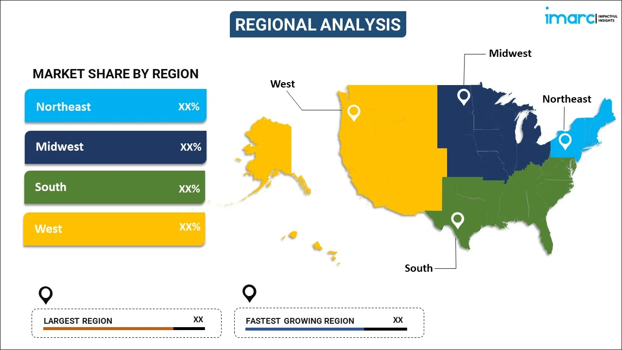
Breakup by Region:
To get detailed regional analysis of this market Request Sample
- Northeast
- Midwest
- South
- West
Competitive Landscape:
The competitive landscape of the industry has also been examined along with the profiles of the key players.
Latest News and Developments:
- In May 2025, Asahi Kasei launched the TA Series of its Sunfort dry film photoresist to support advanced semiconductor packaging, especially for AI, automotive, and IoT applications. Designed for high-resolution patterning with conventional and laser imaging systems, the TA Series enhances wiring precision and production efficiency. This strategic product supports Asahi Kasei’s growth plan and global expansion, addressing increasing industry demand in North America and Asia through tailored technical support.
Report Coverage:
| Report Features | Details |
|---|---|
| Base Year of the Analysis | 2025 |
| Historical Period | 2020-2025 |
| Forecast Period | 2026-2034 |
| Units | Million USD |
| Segment Coverage | Photoresist Type, Photoresist Ancillaries Type, Application, Region |
| Region Covered | Northeast, Midwest, South, West |
| Customization Scope | 10% Free Customization |
| Post-Sale Analyst Support | 10-12 Weeks |
| Delivery Format | PDF and Excel through Email (We can also provide the editable version of the report in PPT/Word format on special request) |
Frequently Asked Questions About the United States Photoresist and Photoresist Ancillaries Market Report
The United States photoresist and photoresist ancillaries market was valued at USD 1,044.6 Million in 2025.
We expect the United States photoresist and photoresist ancillaries market to exhibit a CAGR of 4.28% during 2026-2034.
The rising adoption of photoresist and photoresist ancillaries in manufacturing several consumer devices, such as laptops, smartphones, and multimedia players, is currently driving the United States photoresist and photoresist ancillaries market.
The sudden outbreak of the COVID-19 pandemic had led to the implementation of stringent lockdown regulations across the nation resulting in temporary closure of numerous end use industries for photoresist and photoresist ancillaries.
Based on the photoresist type, the United States photoresist and photoresist ancillaries market can be segmented into ArF immersion, KrF, ArF dry, and g- and i-line. Currently, ArF immersion holds the majority of the total market share.
Based on the photoresist ancillaries type, the United States photoresist and photoresist ancillaries market has been divided into anti-reflective coatings, remover, developer, and others. Among these, anti-reflective coatings exhibit a clear dominance in the market.
Based on the application, the United States photoresist and photoresist ancillaries market can be categorized into semiconductors & ICs, LCDs, printed circuit boards, and others. Currently, semiconductors & ICs account for the largest market share.
On a regional level, the market has been classified into Northeast, Midwest, South, and West, where South currently dominates the United States market.
Need more help?
- Speak to our experienced analysts for insights on the current market scenarios.
- Include additional segments and countries to customize the report as per your requirement.
- Gain an unparalleled competitive advantage in your domain by understanding how to utilize the report and positively impacting your operations and revenue.
- For further assistance, please connect with our analysts.
 Request Customization
 Speak to an Analyst
 Request Brochure
 Inquire Before Buying
Benefits of Customization
- Personalize this research
- Triangulate with your data
- Get data as per your format and definition
- Gain a deeper dive into a specific application, geography, customer, or competitor
- Any level of personalization
Get in Touch With Us
UNITED STATES
Phone: +1-201-971-6302
INDIA
Phone: +91-120-433-0800
UNITED KINGDOM
Phone: +44-753-714-6104
Email: [email protected]
Client Testimonials
.webp)