
Asia Pacific Semiconductor Materials Market Size, Share, Trends and Forecast by Material, Application, End Use Industry, and Country, 2026-2034
Asia Pacific Semiconductor Materials Market Size, Share, Trends & Forecast (2026-2034)
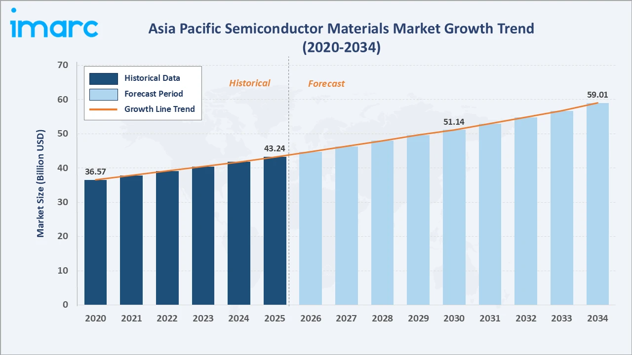
The Asia Pacific semiconductor materials market grew from USD 43.24 Billion in 2025 to USD 44.72 Billion in 2026 and is projected to reach USD 59.01 Billion by 2034, growing at a CAGR of 3.41% during 2026-2034. The market is supported by ongoing wafer fabrication capacity investments across major economies in the region, increasing adoption of advanced semiconductor materials in power electronics and renewable energy applications, and growing requirements for specialty materials in advanced chip packaging. Silicon carbide leads at 35.8% by material type, fabrication dominates at 68.4% by application, and China commands the largest regional share at 42.6% in 2025.
Market Snapshot
|
Metric |
Value |
|
Base Year Market Size (2025) |
USD 43.24 Billion |
|
Market Size (2026) |
USD 44.72 Billion |
|
Forecast Market Size (2034) |
USD 59.01 Billion |
|
CAGR (2026-2034) |
3.41% |
|
Base Year |
2025 |
|
Historical Period |
2020-2025 |
|
Forecast Period |
2026-2034 |
|
Dominant Material |
Silicon Carbide (35.8%, 2025) |
|
Dominant Application |
Fabrication (68.4%, 2025) |
|
Leading Country |
China (42.6%, 2025) |
The Asia Pacific semiconductor materials market grew from USD 36.57 Billion in 2020 to USD 43.24 Billion in 2025, and further to USD 44.72 Billion in 2026, reflecting sustained demand driven by integrated circuit production, advanced chip packaging needs, and the region's dominant position in global semiconductor manufacturing. The market is projected to reach USD 51.14 Billion by 2030 before reaching USD 59.01 Billion by 2034.
To get more information on this market, Request Sample
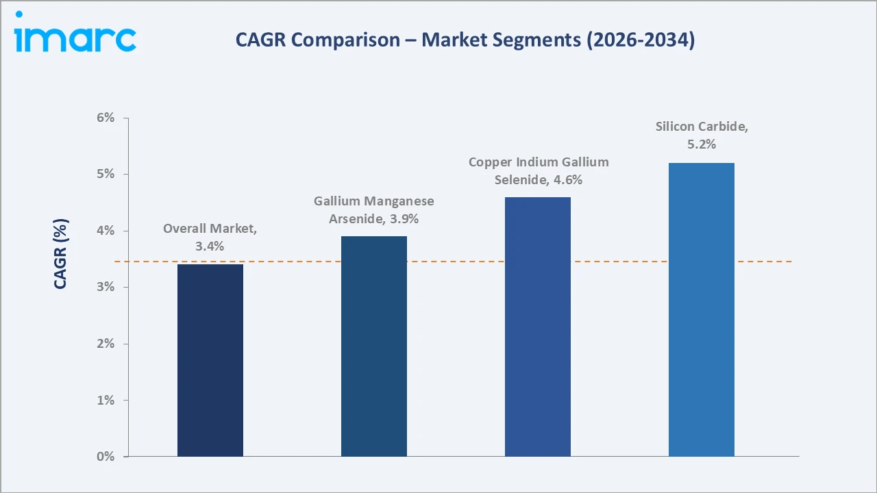
Silicon carbide grows at a 5.2% CAGR as power electronics adoption in electric vehicles and renewable energy systems drives demand for high-performance substrates. Copper indium gallium selenide grows at a 4.6% CAGR, reflecting growing photovoltaic and compound semiconductor applications. Gallium manganese arsenide, at a 3.9% CAGR, is driven by RF and optoelectronic device demand.
Executive Summary
The Asia Pacific semiconductor materials market is on a steady growth trajectory, driven by the region's dominant role in global semiconductor manufacturing, ongoing fab capacity investments across major national semiconductor ecosystems, and growing demand for advanced materials in power electronics, consumer electronics, and telecommunications infrastructure.
Silicon carbide at 35.8% reflects the accelerating adoption of wide-bandgap power semiconductors in automotive, solar, and industrial applications. Fabrication at 68.4% is the dominant application segment, sustained by wafer-level materials demand across advanced logic, memory, and power chip production nodes. China leads regionally at 42.6%, anchored by its scale of semiconductor manufacturing, followed by Japan at 17.8% with a specialty materials supply leadership position.
Key Market Insights
|
Insight |
Data |
|
Dominant Material |
Silicon Carbide – 35.8% share (2025) |
|
Dominant Application |
Fabrication – 68.4% share (2025) |
|
Leading Country |
China – 42.6% (2025) |
|
Key Market Opportunity |
Wide-bandgap material scale-up for power electronics and renewable energy infrastructure creates sustained advanced materials demand across Asia Pacific through 2034. |
Key Analytical Observations Supporting the Above Data:
- Silicon Carbide at 35.8%: SiC dominates because it is the preferred substrate for power electronics, offering superior thermal conductivity and switching efficiency over conventional silicon at high temperatures and voltages, making it essential for EV inverters, solar converters, and industrial drives.
- Fabrication at 68.4%: Fabrication leads because the volume of materials consumed in wafer processing, photoresists, etchants, CMP slurries, deposition gases, and dielectric films vastly exceeds packaging material volumes. The region's dominant fab share sustains consistently high fabrication materials.
- China at 42.6%: China's regional leadership reflects its large-scale semiconductor manufacturing base, domestic IC production growth, and vertically integrated electronics supply chains that generate sustained consumption across all semiconductor material categories.
Asia Pacific Semiconductor Materials Market Overview
The Asia Pacific semiconductor materials market encompasses the production, distribution, and supply of all primary and specialty materials consumed in the manufacture of integrated circuits, discrete semiconductors, power devices, and advanced packaging structures. Core material categories include silicon carbide substrates, compound semiconductor wafers, photoresists, CMP slurries, etchants, chemical vapor deposition precursors, specialty gases, bonding wires, and encapsulants used across chip fabrication and packaging processes.
The market serves a broad ecosystem spanning wafer producers, specialty chemical manufacturers, distributor networks, semiconductor fabricators, integrated device manufacturers, and assembly and test service providers. Growth is supported by sustained government semiconductor investment across major economies, growing electronics demand, and the structural shift toward advanced chip architectures requiring higher-purity, more technically complex materials.
Market Dynamics
To evaluate market opportunities, Request Sample
Market Drivers
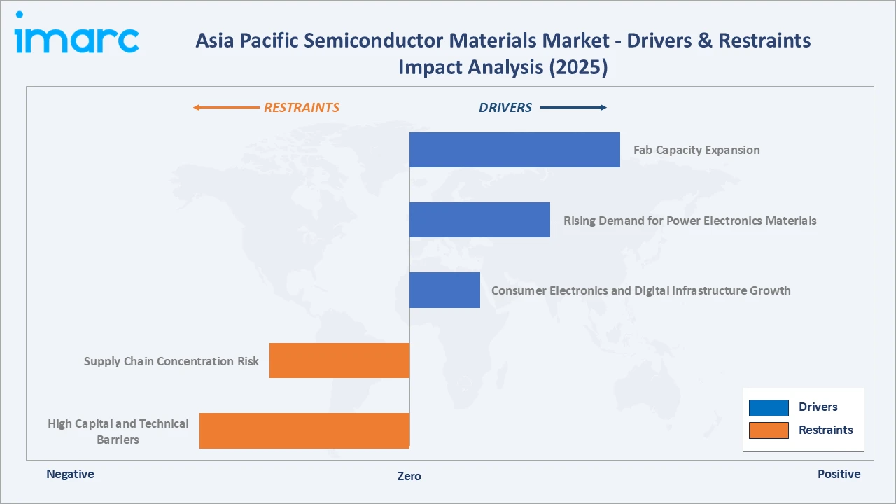
- Fab Capacity Expansion: The Government of India launched the Semicon India Program in January 2022. Within four years, 10 projects worth approximately ₹1.6 lakh crore were approved, with commercial production commencing at Micron and Kaynes facilities, and two additional plants began production in 2026. Substantial fab capacity investment programs across Asia Pacific are supporting sustained demand for wafer materials, specialty chemicals, and process gases across all technology nodes from mature to leading-edge production, creating a broad and durable materials consumption base.
- Rising Demand for Power Electronics Materials: China recorded more than 13 million electric car sales in 2025. In India, electric car sales increased by 75% year-over-year to reach 165,000 units, accounting for nearly 4% of total car sales. Growing adoption of electric vehicles, solar energy systems, and industrial motor drives is increasing demand for wide-bandgap semiconductor substrates and compound semiconductor materials that enable more efficient power conversion and energy management.
- Consumer Electronics and Digital Infrastructure Growth: High-volume consumer electronics manufacturing and expanding digital infrastructure across Asia Pacific generate consistent, large-scale demand for semiconductor materials across wafer, photoresist, etchant, and packaging categories.
Market Restraints
- Supply Chain Concentration Risk: Key precursor materials for compound semiconductors are sourced from limited geographic locations, creating input supply vulnerability and potential production disruptions that can affect manufacturing schedules and overall materials availability in the region.
- High Capital and Technical Barriers: Advanced semiconductor material production requires significant specialized infrastructure, precision equipment, and rigorous quality validation. These barriers limit new entrant capacity additions and constrain rapid supply scaling to meet sudden demand increases.
Market Opportunities
- Wide-Bandgap Material Scale-Up: Accelerating adoption of SiC and GaN power devices creates high-value growth opportunity for substrate producers, epitaxial wafer manufacturers, and compound semiconductor material suppliers as commercialization scales across automotive and energy applications.
- Advanced Packaging Material Demand: The shift to chiplet integration and 3D IC stacking architectures drives new demand for specialty packaging materials with tighter specifications, representing a fast-growing, premium segment within the broader semiconductor materials market.
Market Challenges
- Geopolitical Trade and Export Control Pressures: Expanding export control regimes and trade policy uncertainties affecting advanced materials flows create supply chain fragmentation, compliance cost increases, and technology access barriers for companies operating across the Asia Pacific region.
- Technology Transition Management: Frequent transitions in chip architectures and packaging formats create materials obsolescence risk for specialty producers, requiring continuous research and development investment and rapid product development cycles to maintain qualification at advancing process nodes.
Emerging Market Trends
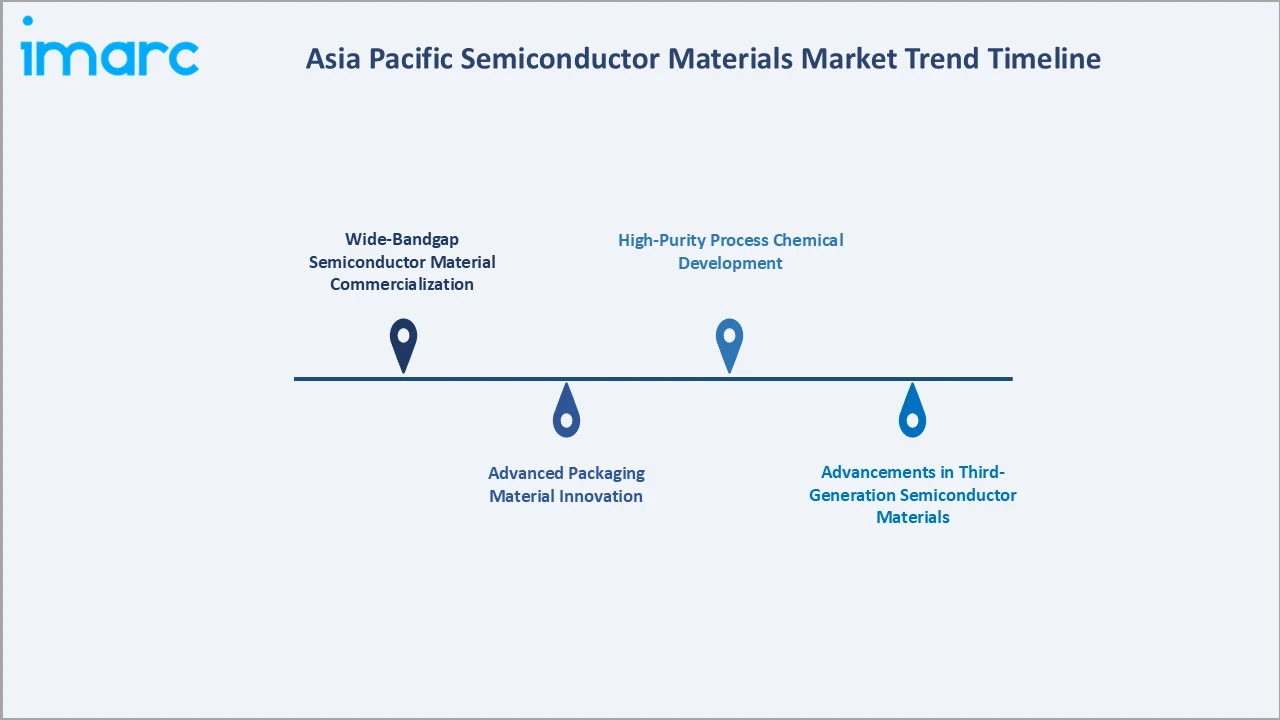
1. Wide-Bandgap Semiconductor Material Commercialization
Silicon carbide and gallium nitride materials are transitioning from specialty to mainstream as automotive and energy sector demand drives adoption at scale. In May 2026, Cyient Semiconductor introduced seven new gallium nitride (GaN) power devices for the domestic market, developed using technology from Navitas Semiconductor, a provider of GaNFast GaN and GeneSiC silicon carbide (SiC) power semiconductors. This transition is reshaping the material composition of the regional semiconductor materials market toward higher-value wide-bandgap substrates.
2. Advanced Packaging Material Innovation
The transition to advanced chip packaging architectures, including 2.5D stacking, fan-out wafer-level packaging, and hybrid bonding, is creating demand for new packaging materials with tighter dimensional and performance specifications. Material suppliers are investing in specialized die attach films, copper interconnect materials, and advanced substrate formulations to serve next-generation packaging platforms that require higher precision and reliability.
3. High-Purity Process Chemical Development
The advancement of lithography and deposition processes at smaller feature sizes is driving development of next-generation photoresist and process chemical formulations with improved sensitivity, resolution, and purity. This trend requires continuous material innovation and close development collaboration between material suppliers and semiconductor manufacturers to qualify new formulations at successive process nodes.
4. Advancements in Third-Generation Semiconductor Materials
In November 2024, Shenzhen launched a national innovation center for third-generation semiconductors to strengthen China's semiconductor self-sufficiency. The facility will support research, design, and prototype production of silicon carbide (SiC) and gallium nitride (GaN) materials and devices. Government-backed innovation centers, domestic semiconductor manufacturing initiatives, and research and development activities are strengthening regional capabilities in semiconductor material design, device development, and prototype production.
Industry Value Chain Analysis
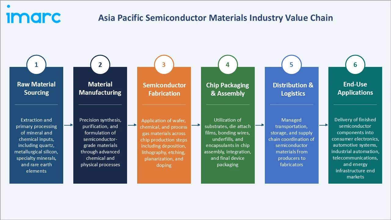
The Asia Pacific semiconductor materials value chain spans six integrated stages from raw material sourcing through end-use applications. Each stage creates value through processing, synthesis, purification, and application.
|
Stage |
Description |
|
Raw Material Sourcing |
Extraction and primary processing of mineral and chemical inputs, including quartz, metallurgical silicon, specialty minerals, and rare earth elements. |
|
Material Manufacturing |
Precision synthesis, purification, and formulation of semiconductor-grade materials through advanced chemical and physical processes. |
|
Semiconductor Fabrication |
Application of wafer, chemical, and process gas materials across chip production steps including deposition, lithography, etching, planarization, and doping. |
|
Chip Packaging & Assembly |
Utilization of substrates, die attach films, bonding wires, underfills, and encapsulants in chip assembly, integration, and final device packaging. |
|
Distribution & Logistics |
Managed transportation, storage, and supply chain coordination of semiconductor materials from producers to fabricators. |
|
End-Use Applications |
Delivery of finished semiconductor components into consumer electronics, automotive systems, industrial automation, telecommunications, and energy infrastructure end markets. |
Material manufacturing is the highest value-added stage, where precision chemical synthesis, ultra-high purity processing, and stringent quality control requirements create durable competitive advantages that are difficult and capital-intensive to replicate. Material manufacturers at this stage invest heavily in research and development to deliver consistent product performance at advancing technology nodes, establishing long-term qualification relationships with semiconductor fabricators.
Technology Landscape in the Asia Pacific Semiconductor Materials Industry
Advanced Photoresist Formulations
The transition to extreme ultraviolet lithography for sub-7nm chip production has driven the development of next-generation chemically amplified photoresist formulations with improved sensitivity and resolution. Metal-oxide photoresist materials are emerging as an advanced EUV resist platform, with ongoing development targeting sub-3nm production node requirements and improving pattern fidelity at tight feature dimensions.
Chemical Mechanical Planarization Innovation
CMP slurry and pad technology advances are enabling planarization of increasingly complex multilayer metal and dielectric stacks in advanced logic and memory chip production. Improved slurry formulations with higher selectivity and refined particle uniformity enable tighter process windows and better yield at advanced production nodes, supporting continued materials demand growth in this segment.
Specialty Gas and Precursor Development
Advances in atomic layer deposition and chemical vapor deposition processes are driving demand for highly pure specialty gas and precursor materials with consistent composition and ultra-low impurity levels. Asia Pacific suppliers are investing in production process upgrades and analytical capabilities to meet increasingly stringent purity and performance specifications from advanced node customers.
Market Segmentation Analysis
The report covers the following segments:
| Segment Category | Leading Segment | Market Share | Year |
|---|---|---|---|
| Material | Silicon Carbide | 35.8% | 2025 |
| Application | Fabrication | 68.4% | 2025 |
| End Use Industry | Consumer Electronics | 🔒 | 2025 |
| Country | China | 42.6% | 2025 |

By Material
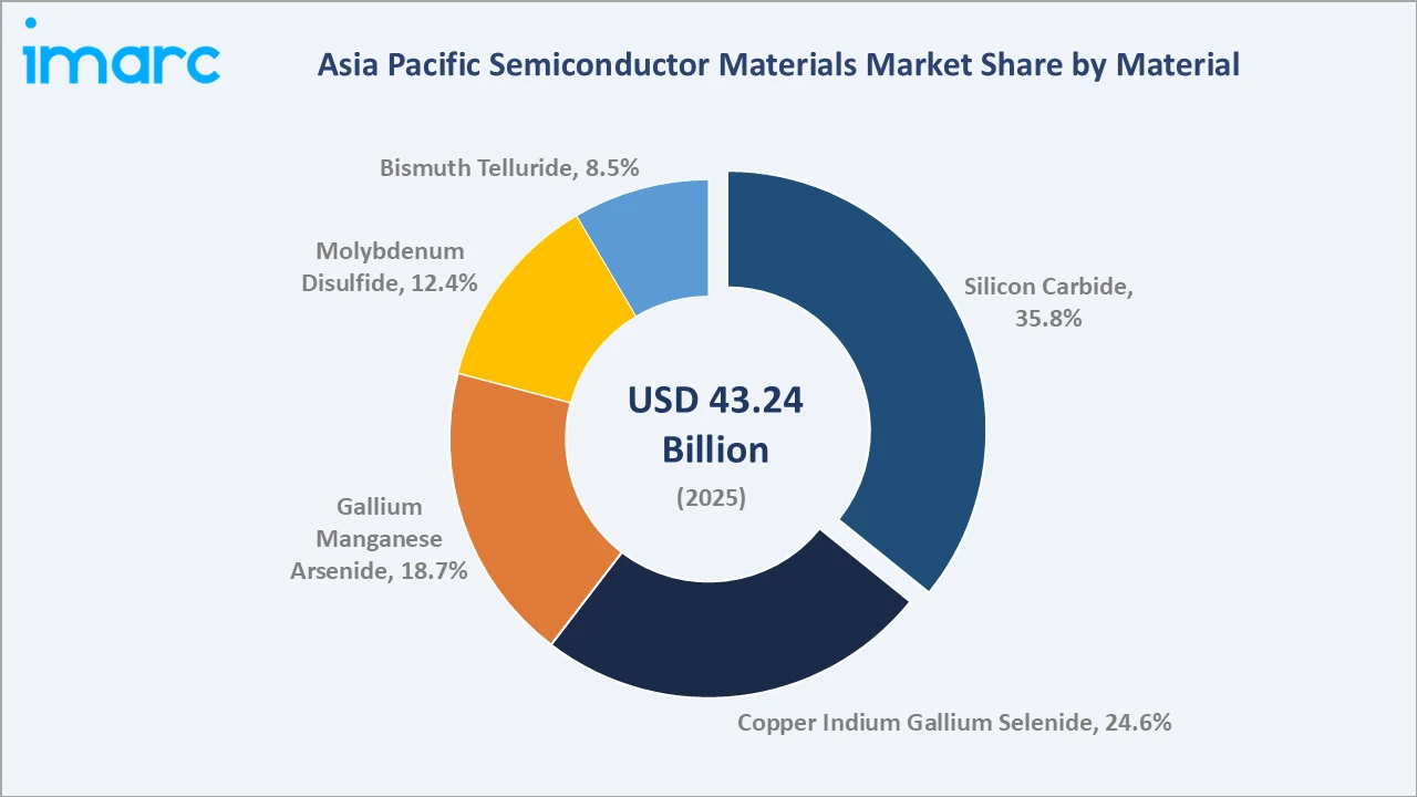
Silicon carbide leads at 35.8% in 2025, reflecting its adoption as the primary substrate for power electronics in automotive, solar, and industrial applications. Its thermal and electrical properties make it the material of choice for high-voltage, high-temperature power device applications where conventional silicon materials are insufficient.
To access detailed market analysis, Request Sample
Copper indium gallium selenide at 24.6% serves photovoltaic thin-film and specialty compound semiconductor applications, with growth supported by renewable energy deployment. Gallium manganese arsenide at 18.7% addresses high-frequency RF, optoelectronic, and magnetic semiconductor requirements. Molybdenum disulfide at 12.4% supports advanced transistor channel and 2D material research applications. Bismuth telluride at 8.5% serves thermoelectric cooling applications in high-performance computing systems.
By Application
Fabrication leads at 68.4% in 2025, driven by the volume of materials consumed across wafer processing, deposition, photolithography, etching, and planarization steps in chip production. The region's dominant share of global wafer fabrication capacity sustains consistently high materials demand in this segment across all technology nodes from mature to leading-edge production.
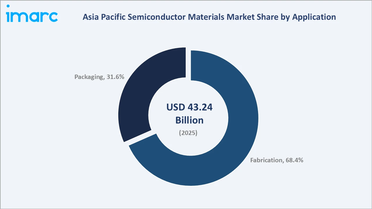
Packaging at 31.6% encompasses all materials used in chip assembly, substrate manufacture, and final device integration. This segment is growing as advanced packaging complexity increases the material content per chip, with heterogeneous integration driving premium substrate and interconnect material demand.
Regional Market Insights
|
Country |
Share (2025) |
Key Characteristics |
|
China |
42.6% |
Domestic IC production growth, state-backed fab investment programs, and vertically integrated electronics supply chains drive sustained, high-volume materials consumption across all categories. |
|
Japan |
17.8% |
Strong position in photoresists, CMP slurries, and epitaxial wafers, with established producer relationships serving global fab customers across advanced and mature technology nodes. |
|
South Korea |
13.9% |
High materials consumption from major memory manufacturing operations and growing advanced packaging activity from leading assembly facilities. |
|
India |
11.6% |
Government semiconductor programs attracting fab investments, progressively building a new semiconductor and materials demand base within Asia Pacific. |
|
Taiwan |
5.7% |
High-purity photoresists, etchants, and specialty gases consumed by leading foundry operations at advanced logic production nodes. |
|
Australia |
4.8% |
Raw material supply contributor. Critical mineral inputs for compound semiconductors and growing advanced materials research activity. |
|
Others |
3.6% |
Emerging semiconductor manufacturing activity across Southeast Asia driving incremental materials demand growth. |
China, at 42.6% of the regional market in 2025, represents the largest semiconductor materials consumption base in Asia Pacific. Japan holds 17.8% of the market and occupies a distinctive position as both a specialty materials producer and a significant consumer. South Korea, at 13.9%, is anchored by its concentration of memory chip production and growing advanced packaging operations.
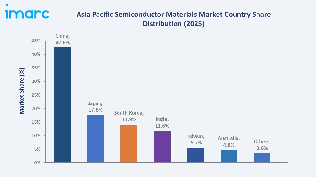
India at 11.6% is the fastest-growing regional contributor, with government semiconductor investment programs supporting the development of new fab and assembly capacity. Taiwan at 5.7% serves as a hub for advanced logic chip production, with specialty materials consumed by leading foundry operations requiring ultra-high purity photoresists, etchants, and process chemicals at sub-5nm production nodes. Australia at 4.8% contributes critical mineral inputs for compound semiconductor manufacturing, supporting upstream material supply across the region. The remaining 3.6% reflects growing semiconductor manufacturing activity across Southeast Asian economies.
Competitive Landscape
The Asia Pacific semiconductor materials market features a mix of large, diversified materials conglomerates and focused specialty producers. Market concentration is highest in silicon wafer and photoresist segments, where established players maintain strong positions through long-term customer qualification requirements, scale advantages, and high technical barriers to entry.
| Company | Key Offerings | Market Position | Core Strength |
|---|---|---|---|
| Shin-Etsu Chemical Co., Ltd. | Silicon Wafers, Compound Semiconductors | Market Leader | One of the largest silicon wafer producers, with a broad materials portfolio across wafer and chemical segments. |
| SUMCO CORPORATION | Polished Wafers, Epitaxial Wafers, Annealed Wafers, Junction Isolated Wafers, Silicon-On-Insulator (SOI) Wafers | Market Leader | SUMCO Corporation plays a major role as a leading manufacturer of high-purity silicon wafers with a massive operational footprint across the Asia Pacific region. |
| Resonac Holdings Corporation | Molding Film, Magnetic Molding Compound for Inductors, Dicing Tape, Thermal Conductive Sheets for Semiconductor Packages | Established Player | Resonac Holdings Corporation acts as a premier leader and critical supplier in the Asia Pacific semiconductor materials market, focusing heavily on back-end packaging processes. |
| Mitsubishi Chemical Group Corporation | Ultrapure synthetic silica powder, Lithomax, aquaSAVE, aquaPASS, Star Series | Established Player | Mitsubishi Chemical Group Corporation acts as a critical specialty materials and high-purity chemical supplier within the APAC semiconductor supply chain. |
| Soulbrain Holdings Co., Ltd. | CVD/ALD materials, CMP Slurry | Challenger | Soulbrain Holdings Co., Ltd. plays a vital role as a key specialized manufacturer and supplier of ultra-high-purity fine chemical materials for the semiconductor industry. |
Competition is intensifying as regional producers expand capabilities across chemical precursors and specialty gases, while established players in wafer and photoresist segments invest in next-generation material innovation to sustain differentiated supply positions and long-term customer qualifications.
Key Company Profiles
Shin-Etsu Chemical Co., Ltd.
Shin-Etsu Chemical Co., Ltd. is a diversified Japanese specialty chemical and materials company with a leading position in silicon wafer production and electronic materials for the semiconductor industry. The company operates across multiple material categories, including substrates, silicones, photomask blanks, and functional chemicals. Its vertically integrated operations and broad product capabilities support a global customer base across semiconductor manufacturing regions.
- Key Offerings: Silicon Wafers, Compound Semiconductors.
- Strategic Focus: Strengthening silicon wafer market leadership through capacity and quality enhancement, while extending capabilities into SiC substrates and advanced photomask materials for next-generation semiconductor production.
SUMCO CORPORATION
SUMCO CORPORATION is a dedicated silicon wafer manufacturer headquartered in Japan, serving wafer requirements for logic, memory, and power device customers globally. The company specializes in large-diameter silicon wafers including polished, epitaxial, and SOI wafer types. Its focused product strategy and precision quality processes support supply relationships with leading semiconductor manufacturers across Asia Pacific and internationally.
- Key Offerings: Polished Wafers, Epitaxial Wafers, Annealed Wafers, Junction Isolated Wafers, Silicon-On-Insulator (SOI) Wafers.
- Strategic Focus: Expanding large-diameter wafer capacity and advancing surface quality standards to support customers at advanced production nodes requiring tighter wafer specification tolerances.
Market Concentration Analysis
The Asia Pacific semiconductor materials market exhibits moderate concentration at the specialty materials segment level, particularly in silicon wafer and photoresist categories where a limited number of established producers hold strong market positions. These segments are characterized by high technical barriers, long-term customer qualification requirements, and significant capital investment thresholds that favor established players over new entrants and support price discipline among leading suppliers.
The broader market, encompassing compound semiconductor materials, specialty gases, etchants, CMP materials, and packaging films, is more fragmented, with multiple producers competing across distinct sub-segments. Growing regional investment in domestic materials production capabilities is gradually increasing competitive intensity in certain commodity material categories, while technical complexity and qualification requirements continue to sustain market concentration in high-specification specialty segments through the forecast period.
Investment & Growth Opportunities
Highest Growth Segments
Silicon carbide grows at 5.2% CAGR, copper indium gallium selenide at 4.6% CAGR, and gallium manganese arsenide at 3.9% CAGR, and these are the highest growth segments.
Investment Themes
- Wide-Bandgap Material Capacity: Accelerating power device adoption across automotive and energy applications creates a compelling investment opportunity in SiC substrate and epitaxial wafer manufacturing in markets where production infrastructure and technical expertise are established.
- Advanced Packaging Materials: Chiplet integration, AI accelerator design, and heterogeneous integration requirements are creating sustained, high-margin growth for specialized packaging material suppliers with the formulation expertise and fab qualification credentials required for advanced platforms.
- Emerging Market Infrastructure: New semiconductor manufacturing investments across India and Southeast Asia are creating greenfield materials demand that offers attractive early-mover positioning for both local producers and established regional suppliers expanding into new geographies.
Future Market Outlook (2026-2034)
The Asia Pacific semiconductor materials market grew from USD 43.24 Billion in 2025 to USD 44.72 Billion in 2026 and is projected to reach USD 59.01 Billion by 2034, exhibiting a CAGR of 3.41% during the forecast period. The market is expected to reach an intermediate milestone of approximately USD 51.14 Billion by 2030, as regional fab capacity expansion programs reach peak ramp phases and demand for advanced logic, memory, and power semiconductor devices continues to grow across end-use applications.
Three structural forces will define the Asia Pacific semiconductor materials market through 2034. First, the ongoing regional fab capacity buildout across China, South Korea, Japan, Taiwan, and India will sustain demand for all categories of wafer, chemical, and specialty materials. Second, accelerating wide-bandgap material commercialization will drive above-market growth in SiC and GaN material categories, reshaping the segment composition of the overall market. Third, the transition to advanced packaging architectures will progressively increase materials complexity and value intensity per chip, expanding the addressable market for specialty packaging material suppliers through the forecast period.
Research Methodology
Primary Research
Primary research comprised structured consultations with semiconductor materials manufacturing executives, fab procurement specialists, advanced packaging engineers, materials distributors, and industry analysts. These discussions validated market sizing estimates, assessed regional demand dynamics, identified segment growth drivers, and provided insights into competitive positioning and technology transition timelines.
Secondary Research
Secondary research drew on semiconductor industry association publications, national government semiconductor strategy documents, company annual reports, trade publications covering semiconductor materials technology, customs and trade flow databases, and independent industry research on fab capacity and materials consumption trends across Asia Pacific economies.
Forecasting Models
Market forecasts used bottom-up and top-down modeling approaches incorporating fab capacity expansion timelines, materials intensity per wafer start, segment growth driver analysis, historical market growth rates, government investment program impact assessments, and macroeconomic indicators including regional GDP growth, electronics output trends, and renewable energy adoption rates affecting wide-bandgap material demand.
Report Coverage:
| Report Features | Details |
|---|---|
| Base Year of the Analysis | 2025 |
| Historical Period | 2020-2025 |
| Forecast Period | 2026-2034 |
| Units | Billion USD |
| Scope of the Report | Exploration of Historical and Forecast Trends, Industry Catalysts and Challenges, Segment-Wise Historical and Predictive Market Assessment:
|
| Materials Covered | Silicon Carbide, Gallium Manganese Arsenide, Copper Indium Gallium Selenide, Molybdenum Disulfide, Bismuth Telluride |
| Applications Covered | Fabrication, Packaging |
| End Use Industries Covered | Consumer Electronics, Manufacturing, Automotive, Energy and Utility, Others |
| Countries Covered | China, Japan, India, South Korea, Australia, Indonesia, Others |
| Companies Covered | Shin-Etsu Chemical Co., Ltd., SUMCO CORPORATION, Resonac Holdings Corporation, Mitsubishi Chemical Group Corporation, Soulbrain Holdings Co., Ltd., etc. |
| Customization Scope | 10% Free Customization |
| Post-Sale Analyst Support | 10-12 Weeks |
| Delivery Format | PDF and Excel through Email (We can also provide the editable version of the report in PPT/Word format on special request) |
Frequently Asked Questions About the Asia Pacific Semiconductor Materials Market Report
The Asia Pacific semiconductor materials market reached USD 44.72 Billion in 2026, driven by fab capacity expansion, wide-bandgap materials demand, and advanced packaging material growth across the region.
The market is forecast at a CAGR of 3.41% during 2026-2034, supported by fab investment programs, SiC material scale-up, and growing advanced packaging material consumption across Asia Pacific.
The market is projected to reach USD 59.01 Billion by 2034, driven by fab capacity growth, power electronics material demand, advanced packaging architectures, and emerging fab ecosystems in India.
Silicon carbide leads with a 35.8% share in 2025, driven by adoption in EV power electronics, solar energy, and industrial motor drive applications requiring wide-bandgap semiconductor materials.
Fabrication leads with a 68.4% share in 2025, driven by high materials consumption in wafer-level chip production across the region's dominant semiconductor fab base.
China leads with a 42.6% share in 2025, reflecting its large-scale semiconductor manufacturing base, domestic IC production growth, and vertically integrated electronics supply chains.
Key players include Shin-Etsu Chemical Co., Ltd., SUMCO CORPORATION, Resonac Holdings Corporation, Mitsubishi Chemical Group Corporation, and Soulbrain Holdings Co., Ltd., among others.
The market is projected to reach approximately USD 51.14 Billion by 2030, driven by fab capacity ramp activity, SiC demand growth, and advanced packaging material expansion across Asia Pacific.
Need more help?
- Speak to our experienced analysts for insights on the current market scenarios.
- Include additional segments and countries to customize the report as per your requirement.
- Gain an unparalleled competitive advantage in your domain by understanding how to utilize the report and positively impacting your operations and revenue.
- For further assistance, please connect with our analysts.
 Request Customization
 Speak to an Analyst
 Request Brochure
 Inquire Before Buying
Benefits of Customization
- Personalize this research
- Triangulate with your data
- Get data as per your format and definition
- Gain a deeper dive into a specific application, geography, customer, or competitor
- Any level of personalization
Get in Touch With Us
UNITED STATES
Phone: +1-201-971-6302
INDIA
Phone: +91-120-433-0800
UNITED KINGDOM
Phone: +44-753-714-6104
Email: [email protected]
Client Testimonials



.webp)




.webp)












Related Reports

Choose your plan
*Please note that the prices mentioned below are starting prices for each bundle type. Kindly contact our team for further details.*
Single User License
- 1 User License, Access on 2 Devices
- PDF Report + Excel Dataset (Password Protected)
- Lifetime Access
- No Printing Rights
- 10% Free Report Customization
- 10–12 Weeks of Analyst Support
Five User License
- Access for 5 Users, 2 Devices per User
- PDF Report + Excel Dataset (Password Protected)
- Lifetime Access
- Dedicated Account Manager
- 12–14 Weeks of Analyst Support
- No Printing Rights
- 15% Free Report Customization
- 25% Discount on Your Next Purchase
Corporate User License
- Unlimited User Access (Within Your Organization)
- PDF Report + Excel Dataset
- Lifetime Access
- Dedicated Account Manager
- 14–20 Weeks of Analyst Support
- No Printing Rights
- 20% Free Report Customization
- 30% Discount on Your Next Purchase
Essential Insights
What's included:
3 reports
- Lifetime Access
- PDF Reports
- Excel Datasets
- 2 Weeks of Free Analyst Support
- 2 User Licenses
- Access on 2 Devices
- Printing Rights
- Complimentary PowerPoint (PPT) Version
- Complimentary License Upgrade
Professional Access
What's included:
5 reports
- Lifetime Access
- PDF Reports
- Excel Datasets
- 8 Weeks of Free Analyst Support
- 2 User Licenses
- Access on 2 Devices
- Printing Rights
- Complimentary PowerPoint (PPT) Version
- Complimentary License Upgrade
Business Advantage
What's included:
8 reports
- Lifetime Access
- PDF Reports
- Excel Datasets
- 14 Weeks of Free Analyst Support
- 2 User Licenses
- Access on 2 Devices
- Printing Rights
- Complimentary PowerPoint (PPT) Version
- Complimentary License Upgrade
Enterprise Intelligence
What's included:
10 reports
- Lifetime Access
- PDF Reports
- Excel Datasets
- 20 Weeks of Free Analyst Support
- 2 User Licenses
- Access on 2 Devices
- Printing Rights
- Complimentary PowerPoint (PPT) Version
- Complimentary License Upgrade