India Silicon Wafer Market Size, Share, Trends and Forecast by Wafer Size, Type, Application, End Use, and Region, 2026-2034
India Silicon Wafer Market Overview:
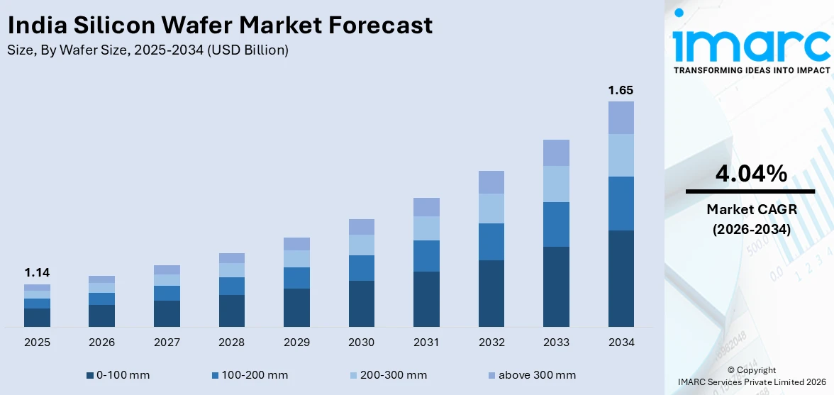
The India silicon wafer market size reached USD 1.14 Billion in 2025. Looking forward, IMARC Group expects the market to reach USD 1.65 Billion by 2034, exhibiting a growth rate (CAGR) of 4.04% during 2026-2034. The increasing demand for semiconductors, government incentives, expansion of electronics manufacturing, 5G and IoT adoption, electric vehicle production, and rising R&D investments in nanotechnology, photovoltaics, and microelectronics across academic and industrial institutions are some of the factors propelling the growth of the market.
|
Report Attribute
|
Key Statistics
|
|---|---|
|
Base Year
|
2025 |
|
Forecast Years
|
2026-2034
|
|
Historical Years
|
2020-2025
|
| Market Size in 2025 | USD 1.14 Billion |
| Market Forecast in 2034 | USD 1.65 Billion |
| Market Growth Rate 2026-2034 | 4.04% |
India Silicon Wafer Market Trends:
Rising Domestic Investment in Silicon Wafer Fabrication
India is experiencing strong movement toward local silicon carbide wafer manufacturing to support the expanding electric mobility and renewable power sectors. New fabrication units are emerging through strategic alliances with global players, backed by state-level support. These facilities are being developed in emerging industrial regions and are aiming for significant output scaling within a short period. The focus is shifting from import dependence to building advanced domestic manufacturing capabilities. The rise of private players in this space also highlights the growing interest in specialized semiconductor infrastructure. With the growing demand for energy-efficient components, local production is expected to play a critical role in meeting industry needs while enhancing India’s position in the global semiconductor value chain. For example, in January 2025, Indichip Semiconductors, in partnership with Japan’s Yitoa Micro Technology, signed an INR 14,000 Crore deal with Andhra Pradesh to establish India’s first private silicon carbide wafer fab in Kurnool. Starting at 10,000 wafers/month, the plant would scale to 50,000 within three years, supporting the EV and renewable energy sectors.
To get more information on this market Request Sample
Strengthening Front-End Semiconductor Fabrication
India is advancing in front-end semiconductor manufacturing with large-scale investments focused on high-capacity wafer fabrication. Backed by government incentives and international technology partnerships, new projects are targeting global demand across automotive, artificial intelligence, computing, and telecommunications. Strategic locations like Gujarat are emerging as key hubs, supported by robust infrastructure and policy frameworks. These developments are not only accelerating local chip production but also creating extensive skilled employment opportunities nationwide. With a substantial monthly output planned, the facilities are designed to integrate cutting-edge process nodes and meet global quality standards. The increasing focus on developing full-stack semiconductor capabilities reflects the broader push to establish India as a competitive and reliable supplier in the global electronics manufacturing ecosystem. For instance, in September 2024, Tata Electronics signed an agreement with the India Semiconductor Mission to set up a semiconductor plant in Dholera, Gujarat, investing INR 910 Billion. The project planned a 50,000 wafers/month capacity and received 50% central funding. Partnering with Powerchip, it aimed to serve global automotive, AI, computing, and communication sectors and generated over 20,000 skilled jobs across India.
India Silicon Wafer Market Segmentation:
IMARC Group provides an analysis of the key trends in each segment of the market, along with forecasts at the region/country level for 2026-2034. Our report has categorized the market based on wafer size, type, application, and end use.
Wafer Size Insights:
- 0-100 mm
- 100-200 mm
- 200-300 mm
- above 300 mm
The report has provided a detailed breakup and analysis of the market based on the wafer size. This includes 0-100 mm, 100-200 mm, 200-300 mm, and above 300 mm.
Type Insights:
- N-Type
- P-Type
A detailed breakup and analysis of the market based on the type have also been provided in the report. This includes N-type and P-type.
Application Insights:
Access the comprehensive market breakdown Request Sample
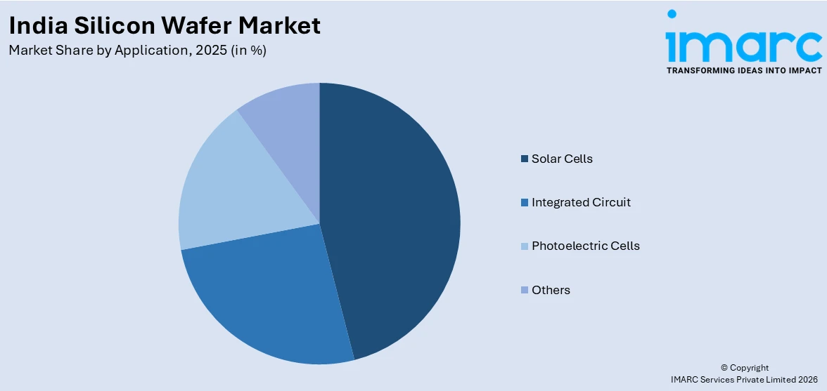
- Solar Cells
- Integrated Circuit
- Photoelectric Cells
- Others
The report has provided a detailed breakup and analysis of the market based on the application. This includes solar cells, integrated circuit, photoelectric cells, and others.
End Use Insights:
- Consumer Electronics
- Automotive
- Industrial
- Telecommunication
- Others
A detailed breakup and analysis of the market based on the end use have also been provided in the report. This includes consumer electronics, automotive, industrial, telecommunication, and others.
Regional Insights:
- North India
- South India
- East India
- West India
The report has also provided a comprehensive analysis of all the major regional markets, which include North India, South India, East India, and West India.
Competitive Landscape:
The market research report has also provided a comprehensive analysis of the competitive landscape. Competitive analysis such as market structure, key player positioning, top winning strategies, competitive dashboard, and company evaluation quadrant has been covered in the report. Also, detailed profiles of all major companies have been provided.
India Silicon Wafer Market News:
- In October 2024, Infineon Technologies developed the world's thinnest silicon power wafer, measuring just 20 micrometers in thickness. This advancement reduces substrate resistance by 50%, leading to over 15% reduction in power loss. The ultra-thin wafers are expected to enhance energy efficiency in various applications, including AI data centers and consumer electronics. This innovation aligns with Infineon's commitment to advancing power semiconductor technology.
India Silicon Wafer Market Report Coverage:
| Report Features | Details |
|---|---|
| Base Year of the Analysis | 2025 |
| Historical Period | 2020-2025 |
| Forecast Period | 2026-2034 |
| Units | Billion USD |
| Scope of the Report |
Exploration of Historical Trends and Market Outlook, Industry Catalysts and Challenges, Segment-Wise Historical and Future Market Assessment:
|
| Wafer Sizes Covered | 0-100 mm, 100-200 mm, 200-300 mm, Above 300 mm |
| Types Covered | N-Type, P-Type |
| Applications Covered | Solar Cells, Integrated Circuit, Photoelectric Cells, Others |
| End Uses Covered | Consumer Electronics, Automotive, Industrial, Telecommunication, Others |
| Regions Covered | North India, South India, East India, West India |
| Customization Scope | 10% Free Customization |
| Post-Sale Analyst Support | 10-12 Weeks |
| Delivery Format | PDF and Excel through Email (We can also provide the editable version of the report in PPT/Word format on special request) |
Key Questions Answered in This Report:
- How has the India silicon wafer market performed so far and how will it perform in the coming years?
- What is the breakup of the India silicon wafer market on the basis of wafer size?
- What is the breakup of the India silicon wafer market on the basis of type?
- What is the breakup of the India silicon wafer market on the basis of application?
- What is the breakup of the India silicon wafer market on the basis of end use?
- What are the various stages in the value chain of the India silicon wafer market?
- What are the key driving factors and challenges in the India silicon wafer market?
- What is the structure of the India silicon wafer market and who are the key players?
- What is the degree of competition in the India silicon wafer market?
Key Benefits for Stakeholders:
- IMARC’s industry report offers a comprehensive quantitative analysis of various market segments, historical and current market trends, market forecasts, and dynamics of the India silicon wafer market from 2020-2034.
- The research report provides the latest information on the market drivers, challenges, and opportunities in the India silicon wafer market.
- Porter's five forces analysis assist stakeholders in assessing the impact of new entrants, competitive rivalry, supplier power, buyer power, and the threat of substitution. It helps stakeholders to analyze the level of competition within the India silicon wafer industry and its attractiveness.
- Competitive landscape allows stakeholders to understand their competitive environment and provides an insight into the current positions of key players in the market.
Need more help?
- Speak to our experienced analysts for insights on the current market scenarios.
- Include additional segments and countries to customize the report as per your requirement.
- Gain an unparalleled competitive advantage in your domain by understanding how to utilize the report and positively impacting your operations and revenue.
- For further assistance, please connect with our analysts.
 Request Customization
 Speak to an Analyst
 Request Brochure
 Inquire Before Buying
Benefits of Customization
- Personalize this research
- Triangulate with your data
- Get data as per your format and definition
- Gain a deeper dive into a specific application, geography, customer, or competitor
- Any level of personalization
Get in Touch With Us
UNITED STATES
Phone: +1-201-971-6302
INDIA
Phone: +91-120-433-0800
UNITED KINGDOM
Phone: +44-753-714-6104
Email: [email protected]
Client Testimonials

.webp)