How to Setup a Semiconductor Manufacturing Business in 2026: Factory Setup Cost
Modern technology relies heavily on semiconductors, which form the core components driving an array of electronic devices—ranging from smartphones and computers to cars and home appliances. Though compact in size, these sophisticated materials are vital for the operation of almost all the technological tools we use every day. In 2024, global semiconductor market size was valued at USD 739.0 Billion, with projections reaching USD 1,265.2 Billion by 2034, at a 5.97% CAGR from 2026-2034.
Recent worldwide disruptions—most notably the semiconductor shortage—have highlighted the critical role of these chips and the intricate networks involved in their production. This guide offers a comprehensive look into how semiconductors are made, tracing the entire process from raw materials to the final silicon chips that power a vast array of devices.
What is a Semiconductor?
Semiconductors possess a distinctive property—they can conduct electricity only under specific conditions—which makes them indispensable to contemporary electronic systems. In contrast to conductors that consistently permit electrical flow, and insulators that resist it, semiconductors can switch between conducting and insulating states based on external influences such as voltage or temperature.
Silicon is the most widely utilized semiconductor material, prized for its plentiful supply, low cost, and excellent electrical characteristics. For specialized, high-performance applications, alternatives such as germanium and gallium arsenide are also employed.
The core function of semiconductors lies in their ability to control electrical current. Through a process called doping, impurities are introduced to alter their conductive properties. This enables semiconductors to form components like transistors, which act as switches to control electrical flow in integrated circuits. These capabilities make semiconductors the foundation of microprocessors, memory chips, and virtually all modern electronic devices.
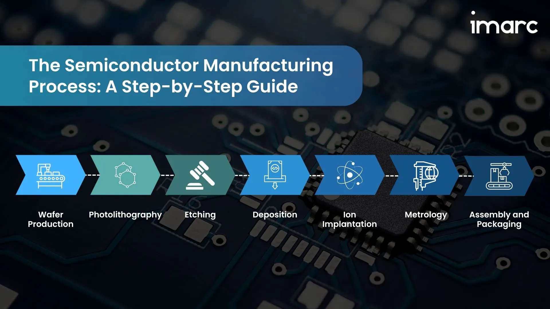
The Semiconductor Manufacturing Process: A Step-by-Step Guide
Semiconductor production is a complex and highly specialized procedure, comprising numerous carefully controlled stages. To achieve optimal chip performance, each phase demands exacting attention to detail. This entire operation takes place in an ultra-clean setting called a cleanroom, located within a semiconductor fabrication facility—commonly referred to as a 'fab.' Below is a summary of the key steps in the process:
- Wafer Production: The process starts with silicon, which is derived from sand. This raw material undergoes purification and is melted down before being formed into a solid single crystal known as an ingot. The ingot is then cut into thin, circular wafers that act as the base upon which semiconductor circuits are constructed.
- Photolithography: Photolithography is a critical step in transferring circuit patterns onto the wafer’s surface. A light-sensitive material, called photoresist, is applied to the wafer. A mask with the circuit pattern is then placed over it, and ultraviolet light is used to expose the photoresist, creating a precise image of the circuit design.
- Etching: After photolithography, the wafer undergoes etching, a process that removes unwanted material to form the intricate patterns of the circuits. This can be done through chemical or plasma etching, with the photoresist protecting areas that should remain intact.
- Deposition: To build the chip’s layers, thin films of various materials are added through deposition techniques such as chemical vapor deposition (CVD) or physical vapor deposition (PVD). These layers form insulating and conductive components necessary for the chip’s functionality.
- Ion Implantation: Ion implantation is used to introduce impurities into the silicon, changing its electrical properties. This process, known as doping, is vital for creating the transistors that form the foundation of the chip’s logic circuits.
- Metrology: Throughout the process, the wafer is carefully inspected and measured using sophisticated tools like electron microscopes and atomic force microscopes. These tools ensure that the circuits are being created to the precise specifications required for high-quality chip performance.
- Assembly and Packaging: Once the circuits are fully developed, the wafer is cut into individual chips, known as dies. Each die is tested for functionality before being packaged in a protective casing. The final chip is then ready to be connected to a circuit board and integrated into electronic devices.
The Machines of the Fab
A semiconductor fabrication plant, or "fab," is one of the most technologically advanced manufacturing environments in the world. Within these facilities, a wide range of sophisticated machines is used to create the intricate patterns and structures necessary for semiconductor chips. These machines, which are both expensive and highly specialized, perform critical tasks throughout the manufacturing process.
- Steppers and Scanners: These are the machines responsible for photolithography. They project intricate circuit patterns onto the silicon wafer using light. Steppers handle individual layers of the chip’s design, while scanners allow for more complex and larger patterns to be printed with high precision.
- Etchers and Cleaners: Etching machines use chemicals or plasmas to carve the wafer’s surface, removing specific material to create circuit patterns. Cleaning machines ensure that the wafers are free from any contaminants that could affect the performance of the chip.
- Deposition Systems: Deposition machines are used to apply thin layers of materials, such as metals or insulators, to the wafer. These systems can work through methods like CVD or PVD to ensure that the layers are applied evenly and accurately.
- Ion Implanters: Ion implantation machines introduce dopants—atoms that alter the semiconductor’s electrical properties—into the wafer. This step is vital for creating the transistors that allow the chip to perform its intended functions.
- Metrology and Inspection Tools: Metrology tools, including electron microscopes and atomic force microscopes, are used to measure and inspect the wafers at various stages. These tools ensure that the features created on the wafer are of the highest precision, as even minor imperfections can affect the chip’s performance.
Beyond the Fab: The Semiconductor Ecosystem
While semiconductor fabs are at the heart of chip production, the semiconductor industry extends far beyond the confines of these manufacturing plants. It is part of a complex, global ecosystem that involves multiple industries, each contributing critical elements to the overall process.
- Electronic Design Automation (EDA) Companies
EDA companies develop the software tools used to design the intricate circuits that are etched onto semiconductor wafers. These tools allow engineers to create highly detailed and precise layouts for the chip’s electrical pathways, optimizing performance and ensuring the final design is functional and efficient.
- Equipment Manufacturers
The machines used in semiconductor fabs—such as steppers, etchers, and ion implanters—are produced by specialized equipment manufacturers. These companies provide the cutting-edge technology necessary for wafer production, ensuring that the tools used in fabs are capable of creating the smallest, most precise features needed for modern chips.
- Raw Material Suppliers
Semiconductor manufacturing relies on a variety of raw materials, primarily high-purity silicon, but also chemicals, gases, and metals required for processes like deposition and etching. Suppliers of these materials ensure that fabs have access to the high-quality substances needed to create reliable, high-performance chips.
- Assembly and Test Companies
Once a wafer is processed and the individual chips are cut, assembly and test companies handle the final stages. These companies package the chips into protective casings and conduct rigorous testing to ensure that each one functions properly before it is sent to customers. The packaging also provides the necessary electrical leads for integrating the chips into electronic devices.
The Future of Semiconductor Manufacturing
The semiconductor industry is continually advancing, driven by the need for smaller, faster, and more efficient chips. As technology progresses, new innovations and manufacturing techniques are being developed to meet these demands. Several emerging trends are poised to shape the future of semiconductor manufacturing.
- Extreme Ultraviolet (EUV) Lithography
EUV lithography represents a significant leap forward in semiconductor manufacturing. This next-generation lithography technology uses extremely short wavelengths of light to create smaller, more precise patterns on the silicon wafer. EUV will enable the production of even smaller and more powerful chips, which is crucial for advancing technologies like artificial intelligence (AI) and 5G networks.
- 3D Packaging
3D packaging involves stacking multiple semiconductor chips on top of one another, creating a more compact and powerful device. This technology allows for greater memory, higher processing power, and better energy efficiency in a smaller footprint. 3D packaging is especially valuable for applications in mobile devices, cloud computing, and data centers.
- New Materials
Researchers are constantly exploring alternative materials to replace or enhance traditional silicon. Materials like graphene, gallium nitride, and others offer superior performance in certain applications, such as faster speeds or greater energy efficiency. The development of these materials could revolutionize semiconductor manufacturing and enable the next generation of high-performance devices.
- Quantum Computing
Quantum computing promises to unlock computational power far beyond what is possible with classical chips. Though still in its early stages, quantum computing research is advancing rapidly, and semiconductors will play a key role in developing the hardware required for quantum systems. This could open new frontiers in fields like cryptography, complex simulations, and artificial intelligence.
Conclusion
Semiconductor manufacturing is a deeply technical and highly refined process that enables much of today’s digital infrastructure. From the initial refinement of silicon to the final stages of packaging and testing, each step relies on advanced machinery, precision control, and global coordination.
The process does not end at the fab; it spans a vast network of industries, from design software and materials to packaging and testing services. Innovations such as EUV lithography, 3D packaging, and new semiconductor materials are already shaping the next generation of devices, pushing performance boundaries and enabling new use cases.
Leverage IMARC’s Expertise in the Semiconductor Industry
IMARC Group offers end-to-end support for companies entering or expanding in the semiconductor market. Our services cover every stage, from planning to execution:
- Manufacturing Plant Project Reports: Turnkey reports with detailed process flows, market analysis, CapEx/OpEx estimates, and ROI projections—providing a complete setup blueprint.
- Market Research & Industry Analysis: In-depth reports on global and regional semiconductor markets, covering trends, forecasts, and key players to support strategic planning.
- Feasibility Studies: Custom assessments of project viability, including technical, financial, and logistical analysis to guide investment decisions.
- Factory Setup Consulting: Support for site selection, regulatory approvals, plant layout design, and supply chain setup to ensure smooth factory launch.
- Procurement & Supply Chain Intelligence: Identification and vetting of suppliers for materials and equipment, focusing on quality, cost, and reliability.
- Competitive Intelligence & Benchmarking: Detailed analysis of key industry players to help refine strategy, improve performance, and identify market gaps.
Our Clients


Contact Us
Have a question or need assistance?
Please complete the form with your inquiry or reach out to us at
Phone Number
+91-120-433-0800+1-201-971-6302
+44-753-714-6104
Previous Post

Process optimization and lean consulting solutions enable companies to streamline operations, eliminate waste, and maximize efficiency in their value chain. Through Lean techniques and continuous improvement practices, we empower organizations to increase productivity, decrease costs, and improve quality, turning operations into competitive strengths.
Explore a step-by-step guide to setting up a paper bag manufacturing plant, including planning, machinery, raw materials, costs, and marketing strategies.
Explore a detailed guide on establishing a manufacturing plant in the UAE, including incentives, legal steps, costs, and strategic industry insights.
In industries where accuracy and compliance are critical, equipment calibration and vendor coordination form the foundation of reliable operations. Whether in production, pharmaceuticals, energy, or research, calibration of equipment ensures accuracy, quality, and compliance with regulatory requirements. At the same time, successful coordination with vendors provides timely service, technical support, and supply chain effectiveness. At IMARC Group, we offer end-to-end calibration and coordination services that help businesses minimize downtime, reduce errors, and maintain operational excellence.
In today's fast-evolving industrial landscape, organizations from various end-use industries are quickly embracing automation and digital monitoring to gain real-time insights, enhance productivity, maintain safety, as well as reduce costs. From smart factories to the digitally enabled energy systems, Industry 4.0 is no longer an option—it is a strategic necessity. Using our services at IMARC Group, we help businesses in identifying, evaluating, as well as implementing tailored automation and digital monitoring solutions that enhance efficiency and long-term sustainability.
Equipment Relocation & Reinstallation services provide secure, efficient, and disruption-minimal transportation of equipment, production lines, and vital assets to new locations. Our turnkey solutions reduce downtime, safeguard precious equipment, and ensure operational readiness after the move, be it for plant growth, site consolidation, or process improvement.
Regulatory approval and licensing entail seeking formal permission from authorities to produce, distribute, or offer products and services in target markets. The procedure depends on the industry, geography, and type of product and may demand careful paperwork, compliance with standards, and extensive testing or inspections.
Explore key steps, incentives, costs, and compliance tips for setting up a manufacturing plant in the US. A complete guide for investors and entrepreneurs.
As industries evolve and operational lifecycles conclude, responsible decommissioning and site closure have become essential components of environmental stewardship and regulatory compliance. Whether it’s an industrial plant, mine, manufacturing unit, or energy facility, decommissioning is not just about shutting down—it's about doing so sustainably, safely, and in alignment with legal and community obligations.
Quality audit services are critical for companies with the objective of upholding high standards, compliance with regulations, and maximizing operational effectiveness. The services entail a rigorous review of processes, products, and systems for purposes of ensuring compliance with quality standards, industry practices, and statutory requirements. Through rigorous audits, firms can detect weaknesses, minimize risks, and undertake remedial measures to better overall performance and customer satisfaction.
Effective spare parts planning and inventory setup are vital for ensuring uninterrupted operations, minimizing downtime, and optimizing costs. Whether you're managing a manufacturing facility, utility infrastructure, or industrial fleet, maintaining the right stock of critical spare parts is essential. At IMARC Group, we help organizations build resilient spare parts strategies through advanced data-driven planning, industry benchmarking, and feasibility assessments.
In today’s highly regulated industrial and commercial environment, Standard Operating Procedures (SOPs) serve as the backbone of compliance, quality, and operational integrity. For businesses across sectors like pharmaceuticals, healthcare, manufacturing, and food processing, adherence to SOPs is not just about maintaining internal discipline—it’s about meeting rigorous external regulatory expectations.
Health and safety compliance audits are organized reviews of workplace conditions, policies, and practices to confirm compliance with occupational safety standards and industry best practices. These audits enable companies to discover potential hazards, reduce risks, and ensure compliance with local and global safety standards, promoting a secure and productive work environment.
Our workforce planning and technical staffing solutions enable companies to create nimble, future-fit teams by linking talent strategies and business goals. We excel at identifying, recruiting, and retaining high-caliber technical talent for operational excellence and innovation in various industries.
Overall Equipment Effectiveness (OEE) is an essential metric used to assess manufacturing efficiency based on the performance of equipment in three significant factors: Availability, Performance, and Quality. Our OEE Improvement Services assist organizations in detecting inefficiencies, removing production losses, and maximizing operational performance to achieve increased productivity and profitability.
In an era defined by rapid industrialization, urban expansion, and climate consciousness, Environmental Impact and Sustainability Studies have emerged as critical tools for responsible decision-making. Governments, investors, and corporations are under growing pressure to adopt sustainable practices that align with global environmental standards. At IMARC Group, we bridge this need by offering comprehensive market intelligence and prefeasibility studies with a dedicated focus on environmental impact and sustainability.
3D modeling and simulation technologies, especially Digital Twins, now serve as laboratories for operational efficiency, product innovation, and predictive maintenance in the era of the digital transformation propelling the industry's evolution. These latest developments permit real-time monitoring and optimization for the lifecycle of any physical asset, system, or process by providing a virtual rendering.
Post-commissioning performance validation is an essential process for guaranteeing that newly commissioned systems, equipment, or facilities are performing as desired, according to design specifications, regulatory requirements, and performance criteria.
Pilot plant setup and evaluation services include designing, building, and running small-volume manufacturing plants for the purpose of testing and proving processes prior to full-scale commercial development. Pilot plant services fill the gap between laboratory experimentation and plant production so that companies can prove technology, determine feasibility, and avoid risk before committing substantial capital.
In today’s dynamic industrial landscape, ensuring the health, safety, and environmental well-being of employees is more critical than ever. Environmental, health, and safety (EHS) training is becoming an essential aspect of responsible corporate practices. It promotes a culture of safety while also guaranteeing adherence to changing regulatory standards. At IMARC Group, we offer customized EHS training solutions aimed at assisting organizations in reducing risk, improving compliance, and fostering robust safety cultures.
In today's dynamic market environment, businesses are under constant pressure to minimize costs, enhance efficiency, and meet customer expectations without overstocking or understocking. At IMARC Group, our Inventory Optimization and Stock Planning Services aim to equip organizations with data-informed insights and practical strategies that effectively align supply with demand.
In today’s fast-paced and highly competitive marketplace, businesses are under increasing pressure to optimize operations, reduce environmental footprints, and comply with evolving regulatory requirements. Equipment Lifecycle Assessment Services (ELAS) offer an all-encompassing method for assessing the efficiency, expenses, ecological effects, and overall sustainability of machinery and equipment for its complete lifespan—from acquisition to disposal.
In today’s hyper-regulated global economy, the difference between a successful market entry and a costly delay often comes down to one word: compliance. Whether you're manufacturing pharmaceuticals, exporting packaged food, or launching consumer electronics, aligning your processes with regulatory standards isn't optional—it's mission-critical.
Multi-vendor coordination and integration services involve the strategic management and seamless unification of multiple vendors, suppliers, and service providers to ensure cohesive operations and optimized performance for your business.
In industries where even the slightest environmental variation can compromise product integrity, the role of clean rooms and cold chain systems becomes paramount. From life-saving pharmaceuticals to temperature-sensitive vaccines and high-precision semiconductors, these operations demand absolute control over air quality and temperature.
In a world where environmental footprint is on the global agenda, waste management has emerged as the defining feature of responsible business and governance. Waste is no longer an afterthought as it used to be. Now it's at the forefront of policy formulation, sustainability reporting, and operational planning.
Establishing a temporary site office and providing utility services requires having fully furnished temporary office facilities with minimal infrastructure to support business operations in remote or project-oriented areas. The establishment of a temporary site office and provision of utility services also provides businesses with an expert working environment that has the necessary utilities, allowing them to focus on temporary work assignments, construction ventures, or expanding into new markets.
In a landmark achievement, India has surpassed Japan to become the world’s fourth-largest economy in 2025, with a nominal GDP of $4.187 trillion, according to the International Monetary Fund (IMF). This milestone, driven by robust growth, strategic reforms, and favorable global conditions, positions India as a global economic powerhouse, trailing only the United States, China, and Germany. As India celebrates this ascent, the nation sets its sights on overtaking Germany to claim the third spot by 2028. Join us as we explore the drivers, implications, and future prospects of India’s economic rise.
In an age defined by resource efficiency, regulatory scrutiny, and rising operational costs, utilities planning is no longer an afterthought—it is a strategic imperative. Whether it's ensuring uninterrupted power in a data center, maintaining air quality in a hospital, or optimizing water and steam systems in a manufacturing plant, intelligent utility planning is the hidden force behind seamless operations.
Raw material sourcing and import advisory services entail the strategic activity of sourcing, screening, and procuring quality raw materials from both local and foreign suppliers. These services help companies obtain cost-effective, dependable, and compliant sources of materials to facilitate smooth production and supply chain operations.
Construction management services, powered by deep market intelligence, provide comprehensive oversight across the entire lifecycle of a construction project—from pre-construction planning to final handover. At IMARC, we integrate data-driven insights into supplier benchmarking, cost forecasting, and regulatory trends to support efficient execution and strategic decision-making.
In a volatile global economy, risk is no longer a question of if but when. Whether it's regulatory changes, supply chain disruptions, cyber attacks, or environmental issues, companies in various industries face uncertainties that can halt growth and profitability. It is here that Risk Assessment and Mitigation Planning Services are no longer a safety measure but a strategic imperative.
Organizations tend to outgrow the facilities that they already have with the fast-paced and ever-changing world of business today. It may be because of growing production requirements, expansion of new markets, or merely maximizing operational efficiencies, facility expansion is always a key component of long-term business planning. Moreover, expanding the facility is not just about expanding space it is about aligning future objectives with infrastructure, reducing risks, and maximizing return on investment.
Vendor auditing and compliance verification are essential procedures for companies that depend on vendors of raw materials and machinery to ensure product quality, operational effectiveness, and regulatory compliance. Vendor auditing is the systematic assessment of vendors to meet specified standards in quality control, financial strength, compliance with laws, and operational dependability. Through careful auditing, companies can manage risks, increase supply chain transparency, and promote long-term, reliable vendor relationships.
In the competitive business environment of the present times, completing projects successfully depends on precise planning and financial management. Project scheduling and cost estimation services are important elements that assist companies in mapping timelines, allocating resources optimally, and estimating project budgets accurately. These services enable organizations to have a systematic mechanism for managing projects, minimizing delays, cost overruns, and scope creep, thereby delivering the project on scheduled time and within the budgeted funds.
In the current competitive and regulation-focused business environment, companies must continuously provide quality, uphold compliance standards, and enhance operational efficiency. A key facilitator for achieving these goals is a Standard Operating Procedure (SOP) - a documented collection of detailed instructions aimed at assisting teams in executing regular tasks reliably and effectively. At IMARC Group, we focus on developing personalized SOPs designed for particular industries and business requirements, guaranteeing your operations stay efficient, adaptable, and compliant.
Installation supervision and equipment commissioning are critical phases in the successful delivery of any capital project. They confirm that equipment, systems, and infrastructure are installed based on technical specifications and run safely and efficiently from their earliest possible start. These services facilitate the identification and rectification of defects early on, cutting down delays, preventing expensive rework, and decreasing long-term operational risks. As industrial projects increase in complexity, proper supervision and formal commissioning are critical to achieve performance goals, comply with regulations, and optimize the return on investment. This process is the basis for dependable, efficient, and safe operations in a broad range of industries.
Contract manufacturer identification services involve the process of locating, evaluating, and selecting reliable manufacturing partners capable of producing goods according to your specifications, quality standards, and business requirements. These services ensure seamless production, cost efficiency, and scalability by identifying manufacturers that align with your operational goals, regulatory compliance, and market demands.
The Bill of Materials (BOM) is a crucial document in the manufacturing process, providing a comprehensive list of all the components, materials, assemblies, and sub-assemblies needed to manufacture a product. BOM preparation services are designed to ensure that every detail of the manufacturing process, from raw materials to finished products, is properly accounted for and organized. At IMARC Group, we offer expert BOM preparation services that help manufacturers streamline production, reduce errors, and optimize costs.
Penetrating new markets is a vital business growth strategy, but it is also fraught with challenges when extending into foreign markets where there are varying regulatory regimes, cultural sensitivities, and business conventions. Perhaps one of the most reliable ways to avoid these challenges is through finding local partners or joint ventures. Local Partner or Joint Venture Identification Services offer companies the necessary assistance required to identify the appropriate local entities that can assist them in overcoming these complexities, driving growth, and realizing operational success in a new market.
On construction and infrastructure projects, on-site delivery of work is a critical aspect to be managed in a manner that projects are delivered on time, within budget, and as per defined quality standards. Site Supervision and Civil Execution Oversight Services aim to ensure that the entire process of construction, starting from planning to execution, adheres to safety requirements, laws, and project specifications. Such services include carefully tracking site work, coordinating contractors, managing resources, and monitoring daily operations to prevent risks and maximize the implementation process.
India and United Kingdom have announced the successful conclusion of a mutually beneficial India – UK Free Trade Agreement (FTA). This forward-looking Agreement is aligned with India’s vision of Viksit Bharat 2047 and complements the growth aspirations of both the countries.
Plant layout and process flow design services optimize the physical arrangement of equipment, workflows, and operational systems within industrial facilities. These services enhance productivity, minimize costs, and ensure seamless material and personnel movement, tailored to your production goals and industry standards.
Procurement Strategy and Cost Benchmarking Services play a pivotal role in optimizing an organization's procurement processes, ensuring that the company gets the best value for its investments. In a world where cost efficiency, sustainability, and strategic sourcing are critical, these services offer businesses the necessary tools to improve their procurement operations and strengthen their competitive position. By offering insights into industry standards, historical data, and best practices, organizations can make informed decisions to streamline their supply chain management, reduce costs, and increase operational efficiency.
In today’s competitive business environment, expanding into new markets or establishing new manufacturing facilities requires careful navigation through local regulations, licensing processes, and government incentives. This is where Industrial Licensing and Incentive Advisory Services come into play. These services guide businesses through the complex regulatory landscape and help them access valuable incentives offered by governments to promote industrial growth.
In today's globalized and competitive market, businesses are constantly seeking ways to improve their supply chain operations. One critical element of a successful supply chain strategy is identifying and evaluating the right suppliers. Supplier Identification and Evaluation Services help businesses find reliable suppliers who can meet their quality, cost, and delivery expectations. At IMARC Group, we offer comprehensive services to guide businesses through the complex supplier selection process, ensuring they partner with the most suitable suppliers to drive efficiency and growth.
Capital Expenditure (CapEx) and Operating Expenditure (OpEx) represent two fundamental pillars of corporate financial management. Capital Expenditure (CapEx) covers investments in assets that fuel future growth—new machinery, property, or digital infrastructure. It builds long-term value, boosts capacity, and often attracts investor confidence.
Starting a new business or expanding an existing one involves substantial risk and investment. To steer through these intricacies, business corporations and entrepreneurs both bank on expert feasibility studies as well as full-fledged business planning services. At IMARC Group, we equip businesses with the insights and strategic tools they require to make informed, data-driven decisions.
Technology transfer services enable the smooth transfer of innovations, knowledge, and technical skills from universities, research institutions, or firms to business enterprises. This enables bridging the innovation-market gap such that advanced technologies are developed, scaled, and commercialized successfully.
In today’s complex project environments, the success of any venture—whether it's an industrial plant, residential development, or large-scale commercial project—largely hinges on the availability and adequacy of utilities and infrastructure. At IMARC Group, we provide utility and infrastructure evaluation services aimed at giving businesses a thorough insight into key support systems that contribute to operational efficiency and project feasibility.
For companies hoping to succeed and last, location analysis and site selection are essential procedures. This service offers a thorough analysis to determine the best geographical areas and sites suited to a client's particular operational requirements and strategic goals. To make sure our recommendations are in complete harmony with your vision, we thoroughly examine your business model, target market, logistical needs, and growth goals.
Distribution partner identification services involve the process of locating, assessing, and selecting reliable and capable partners to distribute your products or services in targeted markets. These services aim to ensure efficient supply chain management, seamless market entry, and expanded business reach by identifying partners that align with your business goals and market requirements.