Saudi Arabia Silicon Wafer Market Size, Share, Trends and Forecast by Wafer Size, Type, Application, End Use, and Region, 2026-2034
Saudi Arabia Silicon Wafer Market Overview:
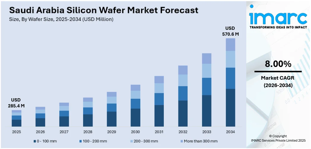
The Saudi Arabia silicon wafer market size reached USD 285.4 Million in 2025. Looking forward, IMARC Group expects the market to reach USD 570.6 Million by 2034, exhibiting a growth rate (CAGR) of 8.00% during 2026-2034. The market is expanding, driven by creation of local infrastructure for the manufacturing of electronic components, government incentives and regulatory frameworks encouraging local content in renewable energy projects, and strategic government investments in research and development (R&D).
|
Report Attribute
|
Key Statistics
|
|---|---|
|
Base Year
|
2025 |
|
Forecast Years
|
2026-2034
|
|
Historical Years
|
2020-2025
|
| Market Size in 2025 | USD 285.4 Million |
| Market Forecast in 2034 | USD 570.6 Million |
| Market Growth Rate 2026-2034 | 8.00% |
Saudi Arabia Silicon Wafer Market Trends:
Innovation in Semiconductor and Electronics Sector
The accelerated development of the electronics industry is the primary driver of silicon wafer demand in Saudi Arabia. Since silicon wafers are the base substrate for microchips and integrated circuits, their demand is directly proportional to the development of these industries. Saudi Arabia is proactively diversifying its economy with Vision 2030, a strategic plan to decrease the nation's reliance on oil by investing in advanced high-tech sectors, such as the production of electronics. This strategic move has driven the creation of local infrastructure for the manufacturing of electronic components, which depends greatly on high-quality silicon wafers. In addition, the increase in the use of smart devices, wearables, and connected consumer electronics is creating the demand for semiconductors, hence fueling the market growth. The IMARC Group predicts that the Saudi Arabia semiconductor market is expected to reach USD 11.1 Billion by 2033. This will further drive the need for silicon wafers.
To get more information on this market, Request Sample
Growth in Renewable Energy Projects, Especially Solar Photovoltaics
Saudi Arabia's renewable energy ambitions are strongly driving the silicon wafer industry, specifically in the solar energy segment. Since they serve as the principal material for solar photovoltaic (PV) cells, silicon wafers are crucial in solar panel production. Moreover, government incentives and regulatory frameworks encouraging local content in renewable energy projects are fostering investment in upstream solar PV materials, including silicon ingots and wafers. These incentives include customs exemptions, subsidies, and long-term purchase agreements for solar energy developers who utilize locally manufactured components. The Kingdom of Saudi Arabia, Middle East has announced its budget plan for 2025, featuring a significant allocation for the energy sector. The proposal allocates 87 Billion Saudi riyals ($23 billion) for the Economic Resources Sector, which includes energy, mining, and industry.
Government Investment in Production and Research and Development (R&D) Infrastructure
Strategic government investments in research and development (R&D), complemented by infrastructure investments in high-end manufacturing, is another critical driver fueling the silicon wafer market in Saudi Arabia. The government has emphasized developing a knowledge-based economy through massive investments in technological innovation, manufacturing clusters, and academic-industry collaboration. Furthermore, the creation of high-tech industrial cities like the Advanced Manufacturing Hub in NEOM provide incentives, such as tax relief, streamlined licensing, and R&D collaboration funding. These environments are meant to entice both local startups and foreign technology companies, generating a self-sustaining market for high-quality semiconductor materials such as silicon wafers. For instance, in 2024, Oxagon, NEOM's industrial pillar, cemented itself as a backbone for manufacturing and logistics, tailored to Saudi Arabia's Vision 2030 with precision. With a combination of innovation, sustainability, and technological advancement, Oxagon emerged as a global example of future industrial growth. Covering around 50 sq. km, it was one of the largest floating industrial complexes globally and was set to reach 100 percent renewable energy consumption by 2030.
Saudi Arabia Silicon Wafer Market Segmentation:
IMARC Group provides an analysis of the key trends in each segment of the market, along with forecasts at the country level for 2026-2034. Our report has categorized the market based on wafer size, type, application, and end use.
Wafer Size Insights:
- 0 - 100 mm
- 100 - 200 mm
- 200 - 300 mm
- More than 300 mm
The report has provided a detailed breakup and analysis of the market based on the wafer size. This includes 0 – 100 mm, 100 - 200 mm, 200 - 300 mm, and more than 300 mm.
Type Insights:
- N-type
- P-type
A detailed breakup and analysis of the market based on the type have also been provided in the report. This includes N-type and P-type.
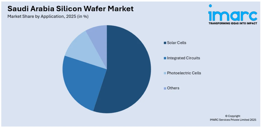
Application Insights:
Access the Comprehensive Market Breakdown, Request Sample
- Solar Cells
- Integrated Circuits
- Photoelectric Cells
- Others
A detailed breakup and analysis of the market based on the application have also been provided in the report. This includes solar cells, integrated circuits, photoelectric cells, and others.
End Use Insights:
- Consumer Electronics
- Automotive
- Industrial
- Telecommunications
- Others
A detailed breakup and analysis of the market based on the end use have also been provided in the report. This includes consumer electronics, automotive, industrial, telecommunications, and others.
Regional Insights:
- Northern and Central Region
- Western Region
- Eastern Region
- Southern Region
The report has also provided a comprehensive analysis of all the major regional markets, which include northern and central region, western region, eastern region, and southern region.
Competitive Landscape:
The market research report has also provided a comprehensive analysis of the competitive landscape. Competitive analysis such as market structure, key player positioning, top winning strategies, competitive dashboard, and company evaluation quadrant has been covered in the report. Also, detailed profiles of all major companies have been provided.
Saudi Arabia Silicon Wafer Market Report Coverage:
| Report Features | Details |
|---|---|
| Base Year of the Analysis | 2025 |
| Historical Period | 2020-2025 |
| Forecast Period | 2026-2034 |
| Units | Million USD |
| Scope of the Report |
Exploration of Historical Trends and Market Outlook, Industry Catalysts and Challenges, Segment-Wise Historical and Future Market Assessment:
|
| Wafer Sizes Covered | 0 – 100 mm, 100 - 200 mm, 200 - 300 mm, More than 300 mm |
| Types Covered | N-type, P-type |
| Applications Covered | Solar Cells, Integrated Circuits, Photoelectric Cells, Others |
| End Uses Covered | Consumer Electronics, Automotive, Industrial, Telecommunications, Others |
| Regions Covered | Northern and Central Region, Western Region, Eastern Region, Southern Region |
| Customization Scope | 10% Free Customization |
| Post-Sale Analyst Support | 10-12 Weeks |
| Delivery Format | PDF and Excel through Email (We can also provide the editable version of the report in PPT/Word format on special request) |
Key Questions Answered in This Report:
- How has the Saudi Arabia silicon wafer market performed so far and how will it perform in the coming years?
- What is the breakup of the Saudi Arabia silicon wafer market on the basis of wafer size?
- What is the breakup of the Saudi Arabia silicon wafer market on the basis of type?
- What is the breakup of the Saudi Arabia silicon wafer market on the basis of application?
- What is the breakup of the Saudi Arabia silicon wafer market on the basis of end use?
- What is the breakup of the Saudi Arabia silicon wafer market on the basis of region?
- What are the various stages in the value chain of the Saudi Arabia silicon wafer market?
- What are the key driving factors and challenges in the Saudi Arabia silicon wafer?
- What is the structure of the Saudi Arabia silicon wafer market and who are the key players?
- What is the degree of competition in the Saudi Arabia silicon wafer market?
Key Benefits for Stakeholders:
- IMARC’s industry report offers a comprehensive quantitative analysis of various market segments, historical and current market trends, market forecasts, and dynamics of the Saudi Arabia silicon wafer market from 2020-2034.
- The research report provides the latest information on the market drivers, challenges, and opportunities in the Saudi Arabia silicon wafer market.
- Porter's five forces analysis assist stakeholders in assessing the impact of new entrants, competitive rivalry, supplier power, buyer power, and the threat of substitution. It helps stakeholders to analyze the level of competition within the Saudi Arabia silicon wafer industry and its attractiveness.
- Competitive landscape allows stakeholders to understand their competitive environment and provides an insight into the current positions of key players in the market.
Need more help?
- Speak to our experienced analysts for insights on the current market scenarios.
- Include additional segments and countries to customize the report as per your requirement.
- Gain an unparalleled competitive advantage in your domain by understanding how to utilize the report and positively impacting your operations and revenue.
- For further assistance, please connect with our analysts.
 Request Customization
 Speak to an Analyst
 Request Brochure
 Inquire Before Buying
Benefits of Customization
- Personalize this research
- Triangulate with your data
- Get data as per your format and definition
- Gain a deeper dive into a specific application, geography, customer, or competitor
- Any level of personalization
Get in Touch With Us
UNITED STATES
Phone: +1-201-971-6302
INDIA
Phone: +91-120-433-0800
UNITED KINGDOM
Phone: +44-753-714-6104
Email: [email protected]
Client Testimonials
.webp)