
Scanning Electron Microscopes Market Size, Share, Trends and Forecast by Type, Technology, Application, and Region, 2026-2034
Scanning Electron Microscopes Market Size, Share, Trends & Forecast (2026-2034)
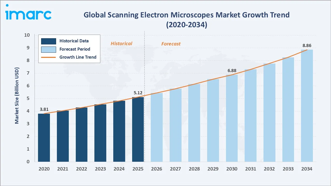
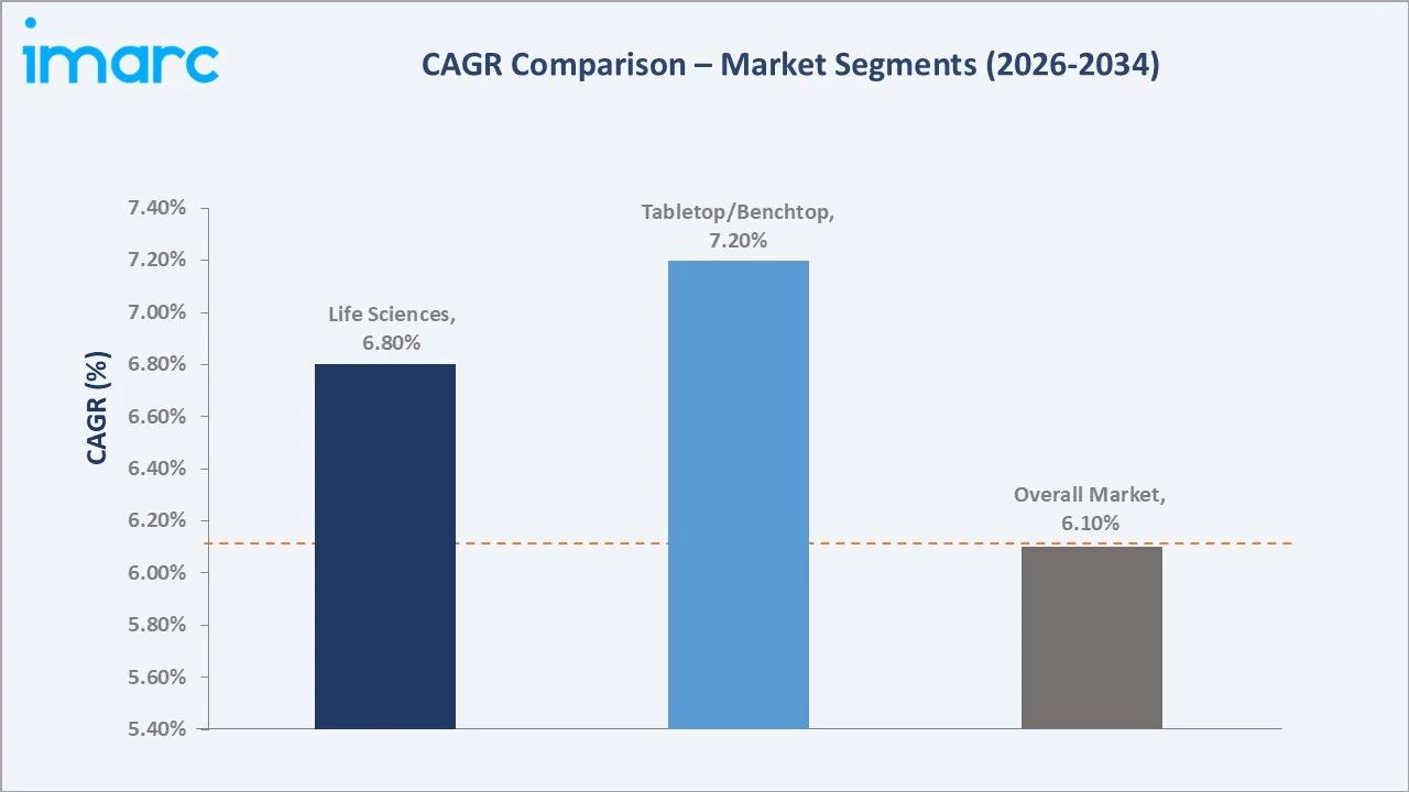
The global scanning electron microscopes market reached USD 5.12 Billion in 2025 and is projected to reach USD 8.86 Billion by 2034, growing at a CAGR of 6.10% during 2026-2034. Expanding semiconductor manufacturing investment, driving process control and failure analysis demand, growing life sciences R&D budgets, accelerating biological imaging applications, nanotechnology research proliferation, and the democratization of electron microscopy through tabletop and benchtop instruments are the primary growth catalysts.
Market Snapshot
|
Metric |
Value |
|
Market Size (2025) |
USD 5.12 Billion |
|
Forecast Market Size (2034) |
USD 8.86 Billion |
|
CAGR (2026-2034) |
6.10% |
|
Base Year |
2025 |
|
Historical Period |
2020-2025 |
|
Forecast Period |
2026-2034 |
Asia-Pacific leads regionally with a 39.8% market share in 2025, anchored by the world’s highest concentration of semiconductor fabrication investment and rapidly expanding pharmaceutical and life sciences R&D capacity across China, Japan, South Korea, and Taiwan. Tabletop/benchtop command the dominant 57.4% type share, reflecting the structural market shift toward compact, user-friendly instruments that have expanded SEM accessibility beyond specialist electron microscopy laboratories to routine quality control, clinical pathology, and undergraduate research applications.
To get more information on this market, Request Sample
The scanning electron microscope market is driven by three structural demand forces: the semiconductor industry’s relentless push to smaller process nodes requiring nanometer-scale imaging and metrology capability that only electron microscopy can provide; the life sciences sector’s growing requirement for nanoscale biological imaging to understand cellular and subcellular structures in drug discovery and pathology; and the broadening of SEM accessibility through tabletop instruments that are expanding the user base well beyond specialized research institutions.
Executive Summary
The global scanning electron microscopes market is experiencing sustained growth, driven by the convergence of semiconductor technology advancement requiring increasingly precise nanoscale metrology, life sciences innovation demanding high-resolution biological imaging, and the democratization of electron microscopy through compact tabletop instruments. The market was valued at USD 5.12 Billion in 2025 and is forecast to reach USD 8.86 Billion by 2034, growing at a CAGR of 6.10%.
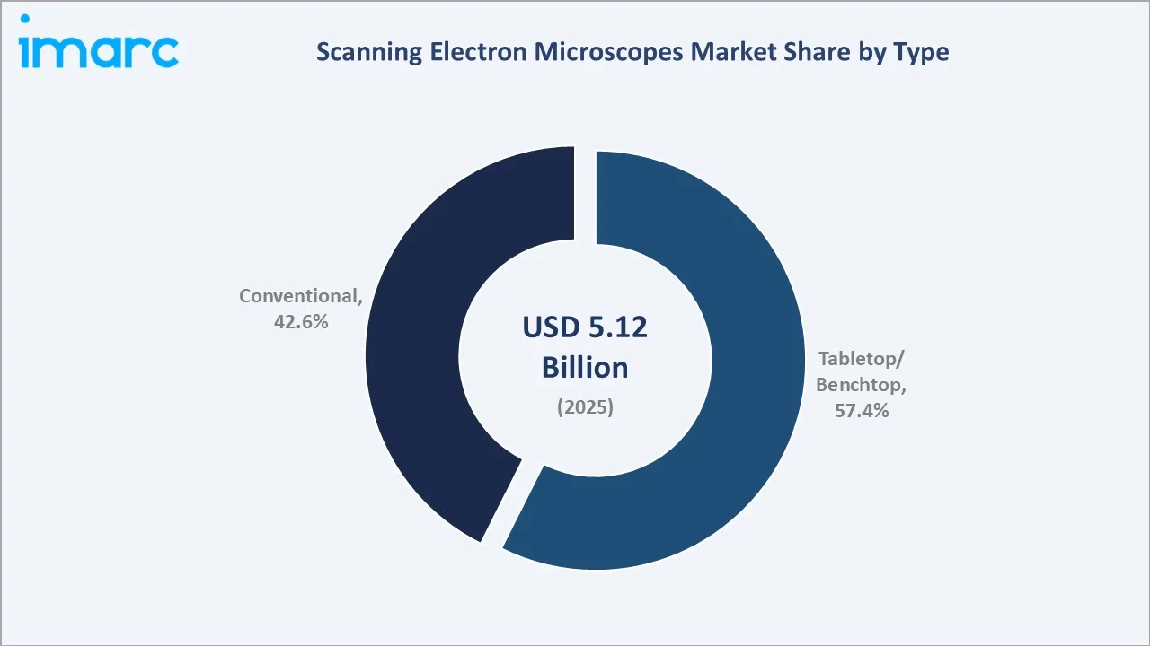
Tabletop/benchtop SEMs account for 57.4% of the type segment in 2025, reflecting the structural market democratization driven by instruments that have reduced SEM purchase price from USD 500,000+ to USD 30,000–150,000, installation footprint from dedicated laboratory rooms to standard bench space, and operational requirement from specialist microscopy training to routine operator competence.
Life sciences at 33.7% represents the largest application segment, reflecting the critical role of SEM in pharmaceutical research, pathology, microbiology, and cell biology applications, where nanoscale structural visualization drives scientific insight and product development.
Asia-Pacific leads regionally at 39.8%, driven by the extraordinary concentration of semiconductor manufacturing investment in Taiwan, South Korea, Japan, and China that collectively accounts for the majority of global advanced wafer fabrication capacity. Key players collectively define the competitive landscape through technological innovation, application expertise, and global service capability.
Key Market Insights
|
Insight |
Data |
|
Largest Type |
Tabletop/Benchtop – 57.4% share (2025) |
|
Second Largest Type |
Conventional – 42.6% share (2025) |
|
Largest Application |
Life Sciences – 33.7% share (2025) |
|
Fastest Growing Application |
Semiconductors – ~7.8% CAGR (2026-2034) |
|
Leading Region |
Asia-Pacific – 39.8% share (2025) |
|
Top Companies |
Thermo Fisher Scientific Inc., Hitachi, Ltd., Carl Zeiss AG, JEOL Ltd. |
Key Analytical Observations Supporting The Above Data:
- Tabletop/benchtop at 57.4% (2025) leads as compact SEM instruments have fundamentally expanded the addressable market by bringing SEM capability to applications and user groups previously excluded by the cost, space, and expertise requirements of conventional floor-standing systems. Quality control laboratories, clinical pathology departments, forensic science units, and undergraduate teaching facilities now routinely deploy SEM as a standard analytical tool.
- Life sciences at 33.7% (2025) reflects the expanding deployment of SEM in pharmaceutical research for nanoparticle characterization and drug delivery system imaging, in clinical pathology for tissue and cellular ultrastructure analysis, and in biological research for cellular membrane, organelle, and microbial structure visualization at nanometer resolution that optical microscopy cannot achieve.
- Semiconductors at 19.4% (2025) is the fastest-growing application segment, driven by the semiconductor industry’s transition to 3nm and below process nodes, where electron beam inspection and metrology are mandatory for defect detection, CD-SEM critical dimension measurement, and failure analysis that cannot be performed with optical inspection tools at these feature dimensions.
- Asia-Pacific’s 39.8% share (2025) reflects the extraordinary concentration of semiconductor capital investment in the region and Japan’s semiconductor renaissance program, collectively deploying hundreds of billions of dollars in new fabrication capacity that requires proportional SEM metrology and inspection tool investment.
Scanning Electron Microscopes Market Overview
A scanning electron microscope is an analytical instrument that uses a focused beam of electrons to scan a sample surface, generating images with nanometer-scale spatial resolution through the detection of secondary electrons, backscattered electrons, and characteristic X-rays. SEM’s unique capability to simultaneously acquire surface morphology images, compositional contrast, and elemental analysis data through integrated EDS (Energy Dispersive X-ray Spectroscopy) and EBSD (Electron Backscatter Diffraction) detectors makes it the standard analytical tool for nanoscale materials characterization across research, quality control, and manufacturing applications.
Macroeconomic drivers include the US companies across the semiconductor ecosystem that have announced more than 140 projects in 30 states, representing over USD 645.3 billion in private investment commitments; top 20 pharmaceutical companies spending an average of USD 8.2 billion on R&D in 2024; and nanotechnology materials R&D growing at above 8% annually as advanced materials find applications in energy, electronics, and healthcare.
Market Dynamics
To evaluate market opportunities, Request Sample
Market Drivers
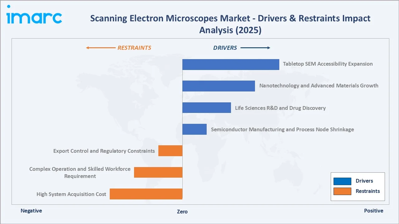
- Semiconductor Manufacturing and Process Node Shrinkage: The semiconductor industry’s continuous advancement to smaller process nodes creates mandatory demand for electron beam inspection and metrology tools. CD-SEM (Critical Dimension SEM) and review SEM systems are indispensable for process control, defect detection, and yield management at advanced nodes where feature dimensions are below the resolution limit of optical inspection.
- Life Sciences R&D and Drug Discovery: Pharmaceutical companies’ expanding investment in nanoparticle drug delivery, cell therapy, and biologics manufacturing requires SEM for nanoparticle size and morphology characterization, formulation quality control, and biological sample imaging at resolutions that reveal subcellular structures relevant to therapeutic mechanism understanding.
- Nanotechnology and Advanced Materials Growth: Nanotechnology research across energy storage, catalysis, additive manufacturing, and composite materials requires SEM as the primary structural characterization tool. The global nanotechnology market, growing at 25.51% from 2026 to 2034, creates proportional SEM demand, with every advanced materials research program requiring SEM imaging capability as a standard analytical resource.
- Tabletop SEM Accessibility Expansion: The commercial success of compact tabletop SEM products costing below USD 100,000 has opened the SEM market to user segments that previously could not justify or accommodate conventional floor-standing SEM systems. This market expansion is structurally additive to the conventional SEM segment, growing the addressable market rather than cannibalizing established high-end system sales.
Market Restraints
- High System Acquisition Cost: Advanced SEM systems, including FIB-SEM workstations and CD-SEM platforms, cost USD 1–5 Million or more, requiring significant capital budgets that are beyond the procurement capacity of smaller academic institutions, SME manufacturing facilities, and research groups in developing economies.
- Complex Operation and Skilled Workforce Requirement: Conventional high-resolution SEM requires specialized training in electron optical system operation, sample preparation techniques including sputter coating and cryo-preparation, image interpretation, and EDS analysis. The shortage of trained electron microscopists in many regions creates an adoption barrier, particularly in emerging economies where the scientific workforce with SEM expertise is limited.
- Export Control and Regulatory Constraints: Advanced electron microscopy systems are subject to export control regulations under multiple national frameworks, including US Export Administration Regulations (EAR) and Wassenaar Arrangement controls, which restrict the sale of high-resolution SEM systems to certain countries and end users.
Market Opportunities
- AI-Powered Automated Image Analysis: The integration of AI and machine learning with SEM imaging systems is enabling automated defect detection, particle classification, and structural measurement that reduces the operator expertise requirement and significantly increases throughput. AI-assisted SEM platforms are attracting adoption in pharmaceutical quality control, semiconductor defect review, and materials characterization applications where high-throughput automated analysis would be commercially transformative.
- Cryo-SEM for Biological Applications: Cryo-scanning electron microscopy, which enables biological samples to be imaged in a near-native hydrated state after rapid cryogenic preparation, is opening new life sciences applications in structural biology, vaccine development, and soft matter characterization.
Market Challenges
- Semiconductor Process Node Transition Complexity: As semiconductor nodes progress below 2nm, the electron beam energies required for SEM imaging risk damaging sensitive photoresist and low-k dielectric materials used in EUV lithography-defined patterns. This beam damage challenge requires instrument manufacturers to develop low-voltage, low-current SEM techniques that maintain image resolution while reducing sample damage.
- Competition from Alternative Nanoscale Characterization Techniques: Atomic force microscopy (AFM), transmission electron microscopy (TEM), and X-ray computed tomography (XCT) provide complementary nanoscale characterization capabilities that compete with SEM in specific application scenarios. This competitive landscape requires SEM manufacturers to continuously differentiate through performance, ease of use, and application-specific capability.
Emerging Market Trends
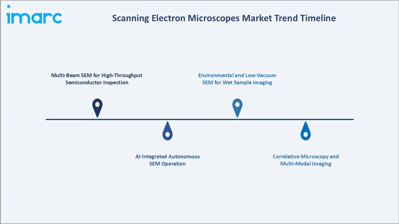
1. Multi-Beam SEM for High-Throughput Semiconductor Inspection
Multi-beam SEM systems using arrays of 9 to 100+ parallel electron beams are transforming semiconductor wafer inspection throughput from the single-beam SEM’s limitation of single-defect review to parallel full-wafer inspection capability. Applied Materials’ eBeam inspection systems and Thermo Fisher’s Helios Hydra PFIB-SEM are addressing the semiconductor industry’s demand for inspection throughput compatible with high-volume manufacturing at EUV lithography nodes.
2. AI-Integrated Autonomous SEM Operation
Leading SEM manufacturers are integrating AI-powered automated operations that perform beam alignment, sample positioning, image acquisition, and analytical measurement without continuous operator input. Thermo Fisher’s Vulcan Automated Lab, launched in 2025, integrates robotic sample handling, AI image analysis, and electron microscopy for semiconductor quality control with minimal human intervention.
3. Correlative Microscopy and Multi-Modal Imaging
Correlative Light and Electron Microscopy (CLEM) workflows that acquire fluorescence microscopy and SEM images of the same sample region are gaining adoption in cell biology research. CLEM enables researchers to identify specific cellular structures by fluorescence labelling and then acquire nanoscale ultrastructural detail by SEM, providing a biological context impossible from either modality alone.
4. Environmental and Low-Vacuum SEM for Wet Sample Imaging
Environmental SEM (ESEM) and low-vacuum SEM technologies enable imaging of hydrated, non-conducting, and beam-sensitive samples, including biological tissues, polymers, and food materials, without conventional preparation, including sputter coating and full dehydration. This capability is expanding SEM adoption in food science, polymer characterization, forensic analysis, and conservation science applications, where traditional sample preparation would damage or alter the sample of interest.
Industry Value Chain Analysis
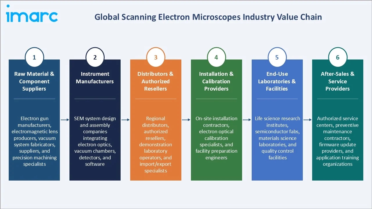
The scanning electron microscope value chain spans from specialized raw material and component suppliers through instrument manufacturing, distribution, installation, and end-use application support. The instrument manufacturing tier is dominated by a small number of specialist electron optical instrument companies with significant proprietary technology in electron gun design, electromagnetic lens fabrication, vacuum system engineering, and detector technology.
|
Stage |
Key Players / Examples |
|
Raw Material & Component Suppliers |
Electron gun manufacturers, electromagnetic lens producers, vacuum system fabricators, suppliers, and precision machining specialists |
|
Instrument Manufacturers |
SEM system design and assembly companies integrating electron optics, vacuum chambers, detectors, and software |
|
Distributors & Authorized Resellers |
Regional distributors, authorized resellers, demonstration laboratory operators, and import/export specialists |
|
Installation & Calibration Providers |
On-site installation contractors, electron optical calibration specialists, and facility preparation engineers |
|
End-Use Laboratories & Facilities |
Life science research institutes, semiconductor fabs, materials science laboratories, and quality control facilities |
|
After-Sales & Service Providers |
Authorized service centers, preventive maintenance contractors, firmware update providers, and application training organizations |
Technology Landscape in the Scanning Electron Microscopes Industry
Electron Optical Column Technology
The core of every SEM is the electron optical column, comprising an electron gun, electromagnetic condenser and objective lenses, beam deflection coils, apertures, and vacuum system. Field emission gun (FEG) technology has replaced thermionic tungsten filament sources as the standard in high-performance SEMs, delivering 5–10× brighter electron beams that enable higher image resolution at lower accelerating voltages, essential for imaging modern semiconductor structures and sensitive biological samples without beam damage.
Detector Technology and Signal Analysis
Modern SEM systems integrate multiple detector types, including secondary electron detectors, backscattered electron detectors, and EDS X-ray detectors for elemental analysis. Next-generation detector systems, including annular multi-detector arrays, enable simultaneous multi-signal acquisition, while EBSD detectors add crystallographic orientation mapping capability. The integration of multiple analytical techniques in a single SEM session, including imaging, elemental mapping, and crystallographic analysis, significantly increases the per-instrument analytical throughput and information yield for operators.
Focused Ion Beam Integration (FIB-SEM)
FIB-SEM systems combine a focused ion beam column with the SEM, enabling simultaneous precision material removal by the ion beam and high-resolution imaging by the electron beam. This combination enables serial section imaging for 3D tomographic reconstruction of materials and biological samples, transmission electron microscopy sample preparation, and precise circuit editing in semiconductor failure analysis. FIB-SEM represents the highest-value segment of the SEM market, with systems including Thermo Fisher’s Helios series priced at USD 1–3 Million.
Market Segmentation Analysis
The report covers the following segments:
|
Segment Category |
Leading Segment |
Market Share |
Year |
|
Type |
Tabletop/Benchtop |
57.4% |
2025 |
|
Application |
Life Sciences |
33.7% |
2025 |
| Technology | Conventional or High Vacuum Scanning Electron Microscope (HVSEM) |
🔒 |
2025 |
|
Region |
Asia-Pacific |
39.8% |
2025 |

By Type
Tabletop/benchtop SEMs lead with a 57.4% share of the global scanning electron microscopes market in 2025, reflecting the transformative market expansion enabled by compact instruments that have made SEM technology accessible to user groups previously excluded by cost, space, and expertise requirements.
To access detailed market analysis, Request Sample
Conventional at 42.6% encompass high-performance floor-standing systems from entry-level analytical SEMs to advanced FIB-SEM workstations. Advanced applications, including semiconductor CD-SEM, FIB cross-section analysis, and cryo-biological imaging, require the performance capabilities of conventional SEM platforms that tabletop instruments cannot replicate.
By Application
Life sciences lead with a 33.7% share in 2025, reflecting the pervasive deployment of SEM across pharmaceutical research, clinical pathology, microbiology, and cell biology. Pharmaceutical companies use SEM for nanoparticle characterization in drug delivery research, characterization of biological particulates and contaminants in quality control, and structural characterization of medical device surfaces.
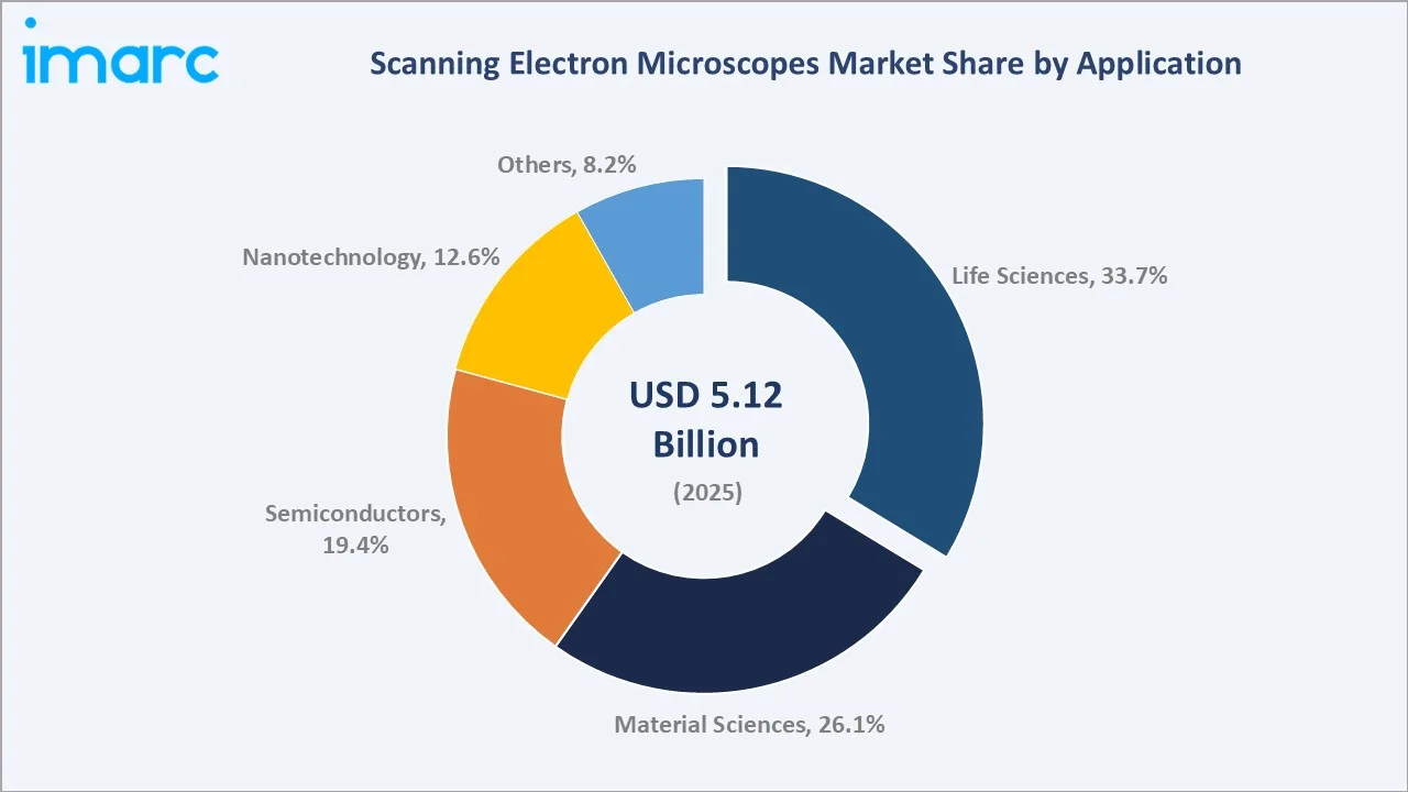
Material sciences at 26.1% reflects SEM’s foundational role in metals, ceramics, polymers, composites, and geological materials characterization for microstructure analysis, failure investigation, and new material development. Semiconductors at 19.4% is the fastest-growing application segment, driven by the semiconductor industry’s transition to 3nm and below process nodes requiring electron beam inspection and metrology at spatial scales optical tools cannot resolve.
Regional Market Insights
Asia-Pacific’s dominant position (39.8%, 2025) reflects the region’s unparalleled concentration of semiconductor manufacturing investment, the world’s largest and fastest-growing pharmaceutical markets in China and Japan, and significant government investment in nanotechnology and advanced materials research across Taiwan, South Korea, Japan, and China.
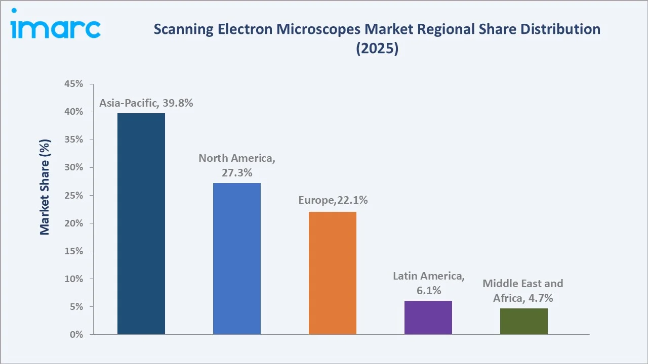
North America, at 27.3%, benefits from the US CHIPS Act-driven domestic semiconductor fab construction program, the world’s largest and most innovative pharmaceutical and biotechnology R&D sector, and strong Department of Defense and National Laboratory investment in advanced materials research and electron microscopy characterization capability.
|
Region |
Share (2025) |
Key Growth Drivers |
|
Asia-Pacific |
39.8% |
World-leading semiconductor manufacturing investments, large and rapidly growing life sciences and pharmaceutical R&D sectors, and expanding material science research capacity |
|
North America |
27.3% |
Strong pharmaceutical and biotechnology R&D investment, leadership in semiconductor technology development, and concentration of world-class research universities |
|
Europe |
22.1% |
Established pharmaceutical and medical device manufacturing base, strong academic research institutions, and European scientific infrastructure investment |
|
Latin America |
6.1% |
Growing university research capacity, increasing pharmaceutical manufacturing R&D investment, and government science funding for nanotechnology |
|
Middle East and Africa |
4.7% |
Emerging research university infrastructure, growing petroleum and petrochemical materials analysis requirements, and expanding healthcare research capacity |
Europe accounts for 22.1% share (2025), driven by pharmaceutical and medical device manufacturing, Airbus aerospace materials research, automotive sector materials quality control, and strong academic electron microscopy infrastructure at research universities. Latin America at 6.1% and the Middle East and Africa at 4.7% represent smaller but growing markets driven by university research capacity building and industrial materials analysis requirements.
Competitive Landscape
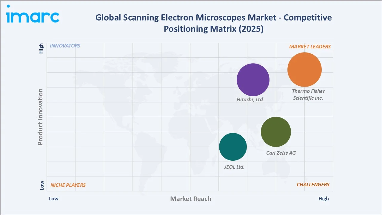
The global scanning electron microscopes market exhibits high concentration at the instrument manufacturer tier, with a small number of specialist electron optical instrument companies accounting for the majority of global market revenue.
|
Company Name |
Product Range |
Market Position |
Core Strength |
|
Thermo Fisher Scientific Inc. |
Apreo ChemiSEM System, Axia ChemiSEM, Verios 5 XHR SEM, Quattro ESEM, Apreo 2 SEM, VolumeScope 2 SEM |
Market Leader |
Broadest SEM portfolio from routine to FIB-SEM, global service network, and deep semiconductor and life science application expertise |
|
Hitachi, Ltd. |
FE-SEM (Field Emission Scanning Electron Microscopes), SEM (Scanning Electron Microscopes), Tabletop Microscopes |
Market Leader |
Large installed base in semiconductor and industrial markets, strong Asia-Pacific position, and competitive tabletop SEM range |
|
Carl Zeiss AG |
Sigma, GeminiSEM, MultiSEM, EVO Family |
Strong Challenger |
High-resolution optics leadership, strong academic and materials science customer base, and innovative correlative microscopy platforms |
|
JEOL Ltd. |
JSM-IT, JCM-7000 NeoScope Benchtop SEM, LazEdge Laser SEM system |
Strong Challenger |
Broad SEM product range, strong relationships with academic and industrial users, and competitive environmental SEM capability |
The competitive dynamics of the SEM market are shaped by long product development cycles, high switching costs for established laboratory users, and the technical depth required to develop and manufacture competitive electron optical systems.
Key Company Profiles
Thermo Fisher Scientific Inc.
Thermo Fisher Scientific Inc. is one of the world’s largest scientific instrument companies and the global leader in electron microscopy through its Materials and Structural Analysis division.
- Product Portfolio: Apreo ChemiSEM System, Axia ChemiSEM, Verios 5 XHR SEM, Quattro ESEM, Apreo 2 SEM, and VolumeScope 2 SEM.
- Recent Developments: In July 2025, Thermo Fisher Scientific Inc. launched the Scios 3 FIB-SEM and Talos 12 TEM electron microscopes at M&M 2025. The systems improve research accessibility through automation, easier workflows, smaller footprints, and advanced imaging for materials science, biology, pathology, and drug development.
- Strategic Focus: AI-powered automated SEM for semiconductor manufacturing; life sciences cryo-EM expansion; multi-beam SEM for high-throughput wafer inspection; EV battery materials characterization workflow development.
Hitachi, Ltd.
Hitachi, Ltd.’s subsidiary Hitachi High-Tech Corporation is one of the world’s largest SEM manufacturers and one of the leading providers of semiconductor CD-SEM measurement systems globally.
- Product Portfolio: FE-SEM (Field Emission Scanning Electron Microscopes), SEM (Scanning Electron Microscopes), and Tabletop Microscopes.
- Recent Developments: In October 2025, Hitachi High-Tech Corporation launched the SU9600 ultrahigh-resolution scanning electron microscope for sub-nano-level observation. It improves high-throughput data acquisition through automated imaging and data-handling workflows for semiconductors, electronics, and advanced materials.
- Strategic Focus: Semiconductor CD-SEM market leadership; tabletop SEM market penetration through TM and FlexSEM series; AI-based measurement automation for semiconductor inspection throughput enhancement.
Market Concentration Analysis
The global SEM market exhibits high concentration, with the top manufacturers collectively accounting for approximately 60–65% of global market revenue. The remaining share of market revenue is distributed among specialist manufacturers, serving specific geographic markets or application niches.
The high concentration of the SEM market reflects the significant technical and capital barriers to developing competitive electron optical systems, field emission gun fabrication, electromagnetic lens design, ultra-high vacuum engineering, and detector development, each of which requires specialized engineering capability built over decades. These barriers have prevented the commoditization that characterizes less technically complex scientific instrument categories, maintaining premium pricing and above-average margins for established SEM manufacturers.
Investment & Growth Opportunities
Fastest Growing Segments
Semiconductors (~7.8% CAGR), EV battery materials characterization SEM applications (~9% annual growth), and AI-automated SEM platforms represent the highest-growth investment vectors within the SEM market through 2034. Cryo-SEM for life sciences, particularly in structural biology and vaccine development, is growing at above 8% CAGR as the technique transitions from specialized research tool to pharmaceutical industry standard characterization method.
Emerging Application Opportunities
EV battery materials characterization represents one of the most significant emerging SEM application opportunities. Battery manufacturers require SEM for electrode microstructure analysis, electrolyte-electrode interface characterization, lithium dendrite failure analysis, and solid-state electrolyte material development – applications that are driving new SEM acquisitions at battery R&D centers and gigafactory quality control laboratories globally.
Technology Investment Trends
- AI integration for automated SEM operation, defect classification, and measurement automation is attracting R&D investment from all major SEM manufacturers as the semiconductor industry demands higher throughput and reduced operator intervention for 24/7 manufacturing quality control deployments.
- Cryo-SEM technology development for native-state biological and soft matter imaging is attracting investment from pharmaceutical and biotech company partnerships with SEM manufacturers, driven by the FDA’s increasing requirement for nanoparticle characterization in biologics and nanoparticle drug regulatory submissions.
Future Market Outlook (2026-2034)
The global scanning electron microscopes market is positioned for sustained growth through 2034. From USD 5.12 Billion in 2025, the market is projected to reach USD 8.86 Billion by 2034, representing total incremental value creation of USD 3.74 Billion at a CAGR of 6.10%.
This growth is underpinned by the semiconductor industry’s multi-decade roadmap for continued node scaling, requiring increasingly sophisticated electron beam inspection tools, the pharmaceutical industry’s expanding nanotechnology drug delivery pipeline requiring nanoscale characterization, and the continued democratization of SEM capability through tabletop instruments that are expanding the instrument’s user base.
The market’s technology evolution will be shaped by AI integration, multi-beam electron optics, and in-situ environmental capabilities that extend SEM from static imaging to dynamic process observation. SEM instruments are progressively transitioning from specialist laboratory tools requiring expert operation to automated analytical platforms deployable in manufacturing quality control environments by non-specialist operators, a transition that will significantly expand the addressable market beyond the current core of research laboratories and semiconductor fabs.
Research Methodology
Primary Research
Primary research comprised structured interviews with over 65 industry participants in 2024–2025, including SEM instrument manufacturers, electron microscopy laboratory directors, semiconductor process control engineers, pharmaceutical analytical scientists, materials characterization specialists, and university microscopy facility managers. Expert input validated market sizing, segment growth rates, and regional penetration estimates.
Secondary Research
Secondary research encompassed SEM manufacturer annual reports and investor presentations, Microscopy Society of America technical publications, Royal Microscopical Society journal data, SEMI semiconductor equipment market statistics, FDA guidance documents on nanoparticle characterization, European Research Council grant data on electron microscopy, and industry publications including Microscopy Today, Journal of Microscopy, and Ultramicroscopy.
Forecasting Models
Market size estimations were derived using top-down and bottom-up forecasting, incorporating SEM instrument unit shipment data by category and geography, average selling price trend analysis by instrument type, end-user segment R&D and capital expenditure budget projections, and semiconductor equipment investment cycle modelling. The base-case CAGR of 6.10% reflects consensus estimates validated against instrument manufacturer revenue guidance and semiconductor, pharmaceutical, and materials R&D investment projections for 2026–2034.
Scanning Electron Microscopes Market Report Scope:
| Report Features | Details |
|---|---|
| Base Year of the Analysis | 2025 |
| Historical Period | 2020-2025 |
| Forecast Period | 2026-2034 |
| Units | Billion USD |
| Scope of the Report | Exploration of Historical Trends and Market Outlook, Industry Catalysts and Challenges, Segment-Wise Historical and Future Market Assessment:
|
| Types Covered | Tabletop/Benchtop, Conventional |
| Technologies Covered | Conventional or High Vacuum Scanning Electron Microscope (HVSEM), Variable Pressure or Low Vacuum Scanning Electron Microscope (LVSEM), Cryo-Scanning Electron Microscope (Cryo-SEM), Environmental Scanning Electron Microscope (ESEM), Others |
| Applications Covered | Material Sciences, Nanotechnology, Life Sciences, Semiconductors, Others |
| Regions Covered | Asia Pacific, Europe, North America, Latin America, Middle East and Africa |
| Countries Covered | United States, Canada, Germany, France, United Kingdom, Italy, Spain, Russia, China, Japan, India, South Korea, Australia, Indonesia, Brazil, Mexico |
| Companies Covered | Thermo Fisher Scientific Inc., Hitachi Ltd., Carl Zeiss AG, JEOL Ltd., etc. |
| Customization Scope | 10% Free Customization |
| Post-Sale Analyst Support | 10-12 Weeks |
| Delivery Format | PDF and Excel through Email (We can also provide the editable version of the report in PPT/Word format on special request) |
Key Benefits for Stakeholders:
- IMARC’s industry report offers a comprehensive quantitative analysis of various market segments, historical and current market trends, market forecasts, and dynamics of the scanning electron microscopes market from 2020-2034.
- The research report provides the latest information on the market drivers, challenges, and opportunities in the global scanning electron microscopes market.
- The study maps the leading, as well as the fastest-growing, regional markets. It further enables stakeholders to identify the key country-level markets within each region.
- Porter's five forces analysis assists stakeholders in assessing the impact of new entrants, competitive rivalry, supplier power, buyer power, and the threat of substitution. It helps stakeholders to analyze the level of competition within the scanning electron microscopes industry and its attractiveness.
- The competitive landscape allows stakeholders to understand their competitive environment and provides insight into the current positions of key players in the market.
Frequently Asked Questions About the Scanning Electron Microscopes Market Report
The global scanning electron microscopes market reached USD 5.12 Billion in 2025 and is projected to reach USD 8.86 Billion by 2034.
The market is expected to grow at a CAGR of 6.10% during 2026-2034, driven by semiconductor manufacturing demand, life sciences R&D expansion, nanotechnology research growth, and tabletop SEM market democratization.
Asia-Pacific leads with a 39.8% share in 2025, driven by the world’s highest concentration of semiconductor manufacturing investment, large pharmaceutical and life sciences R&D sectors, and significant government-funded nanotechnology and materials research programs.
Tabletop/benchtop lead with a 57.4% share in 2025, reflecting the structural market expansion enabled by compact, affordable instruments that have brought SEM capability to quality control, educational, and clinical laboratory applications previously served by optical microscopy alone.
Life sciences lead with a 33.7% share in 2025, encompassing pharmaceutical nanoparticle characterization, clinical pathology ultrastructural analysis, microbiology, and cell biology research applications requiring nanometer-scale imaging resolution.
Some of the key players include Thermo Fisher Scientific Inc., Hitachi, Ltd., Carl Zeiss AG, and JEOL Ltd.
Key drivers include semiconductor manufacturing transition to 3nm and below process nodes requiring electron beam inspection and CD-SEM metrology, nanotechnology and advanced materials research growth, and tabletop SEM democratization, expanding the market to new user segments.
Key opportunities include multi-beam SEM for semiconductor wafer inspection, AI-automated SEM platforms for manufacturing quality control, EV battery materials characterization workflows, and FIB-SEM for 3D materials and biological sample tomography.
Need more help?
- Speak to our experienced analysts for insights on the current market scenarios.
- Include additional segments and countries to customize the report as per your requirement.
- Gain an unparalleled competitive advantage in your domain by understanding how to utilize the report and positively impacting your operations and revenue.
- For further assistance, please connect with our analysts.
 Request Customization
 Speak to an Analyst
 Request Brochure
 Inquire Before Buying
Benefits of Customization
- Personalize this research
- Triangulate with your data
- Get data as per your format and definition
- Gain a deeper dive into a specific application, geography, customer, or competitor
- Any level of personalization
Get in Touch With Us
UNITED STATES
Phone: +1-201-971-6302
INDIA
Phone: +91-120-433-0800
UNITED KINGDOM
Phone: +44-753-714-6104
Email: [email protected]
Client Testimonials




.webp)




.webp)













Related Reports

Choose your plan
*Please note that the prices mentioned below are starting prices for each bundle type. Kindly contact our team for further details.*
Single User License
- 1 User License, Access on 2 Devices
- PDF Report + Excel Dataset (Password Protected)
- Lifetime Access
- No Printing Rights
- 10% Free Report Customization
- 10–12 Weeks of Analyst Support
Five User License
- Access for 5 Users, 2 Devices per User
- PDF Report + Excel Dataset (Password Protected)
- Lifetime Access
- Dedicated Account Manager
- 12–14 Weeks of Analyst Support
- No Printing Rights
- 15% Free Report Customization
- 25% Discount on Your Next Purchase
Corporate User License
- Unlimited User Access (Within Your Organization)
- PDF Report + Excel Dataset
- Lifetime Access
- Dedicated Account Manager
- 14–20 Weeks of Analyst Support
- No Printing Rights
- 20% Free Report Customization
- 30% Discount on Your Next Purchase
Essential Insights
What's included:
3 reports
- Lifetime Access
- PDF Reports
- Excel Datasets
- 2 Weeks of Free Analyst Support
- 2 User Licenses
- Access on 2 Devices
- Printing Rights
- Complimentary PowerPoint (PPT) Version
- Complimentary License Upgrade
Professional Access
What's included:
5 reports
- Lifetime Access
- PDF Reports
- Excel Datasets
- 8 Weeks of Free Analyst Support
- 2 User Licenses
- Access on 2 Devices
- Printing Rights
- Complimentary PowerPoint (PPT) Version
- Complimentary License Upgrade
Business Advantage
What's included:
8 reports
- Lifetime Access
- PDF Reports
- Excel Datasets
- 14 Weeks of Free Analyst Support
- 2 User Licenses
- Access on 2 Devices
- Printing Rights
- Complimentary PowerPoint (PPT) Version
- Complimentary License Upgrade
Enterprise Intelligence
What's included:
10 reports
- Lifetime Access
- PDF Reports
- Excel Datasets
- 20 Weeks of Free Analyst Support
- 2 User Licenses
- Access on 2 Devices
- Printing Rights
- Complimentary PowerPoint (PPT) Version
- Complimentary License Upgrade