
Semiconductor Foundry Market Size, Share, Trends and Forecast by Technology Node, Foundry Type, Application, and Region, 2026-2034
Global Semiconductor Foundry Market Size, Share, Trends & Forecast (2026-2034)
The global semiconductor foundry market was valued at USD 91.20 Billion in 2025 and is projected to reach USD 141.40 Billion by 2034, expanding at a CAGR of 4.83% during the forecast period (2026-2034). Demand is propelled by surging AI and HPC chip requirements, global 5G network rollouts, with the total number of 5G connections globally surpassed 2.7 billion by 2025, automotive electrification, and the unprecedented government investment in domestic semiconductor manufacturing triggered by geopolitical supply chain restructuring. IDMs command 63.7% market share (2025), while communication applications lead at 35.4%. Asia Pacific dominates with a 71.2% regional share.
Market Snapshot
|
Metric |
Value |
|
Market Size (2025) |
USD 91.20 Billion |
|
Forecast Market Size (2034) |
USD 141.40 Billion |
|
CAGR (2026-2034) |
4.83% |
|
Base Year |
2025 |
|
Historical Period |
2020-2025 |
|
Forecast Period |
2026-2034 |
|
Largest Region |
Asia Pacific (71.2%, 2025) |
|
Fastest Growing Region |
North America (CAGR ~7.2%, 2026-2034) |
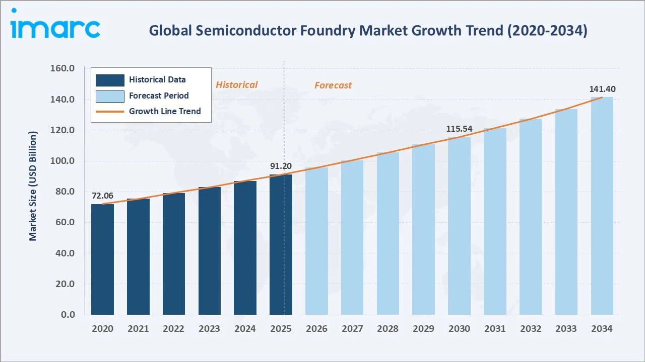
The global semiconductor foundry market from 2020 through 2034, starting at USD 72.06 Billion in 2020 amid chip shortages triggered by COVID-19 supply disruptions, the market advanced to USD 91.20 Billion in 2025. The market is projected to cross USD 115.54 Billion by 2030 before reaching USD 141.40 Billion in 2034, driven by sustained AI, automotive, and advanced node semiconductor demand.
To get more information on this market, Request Sample
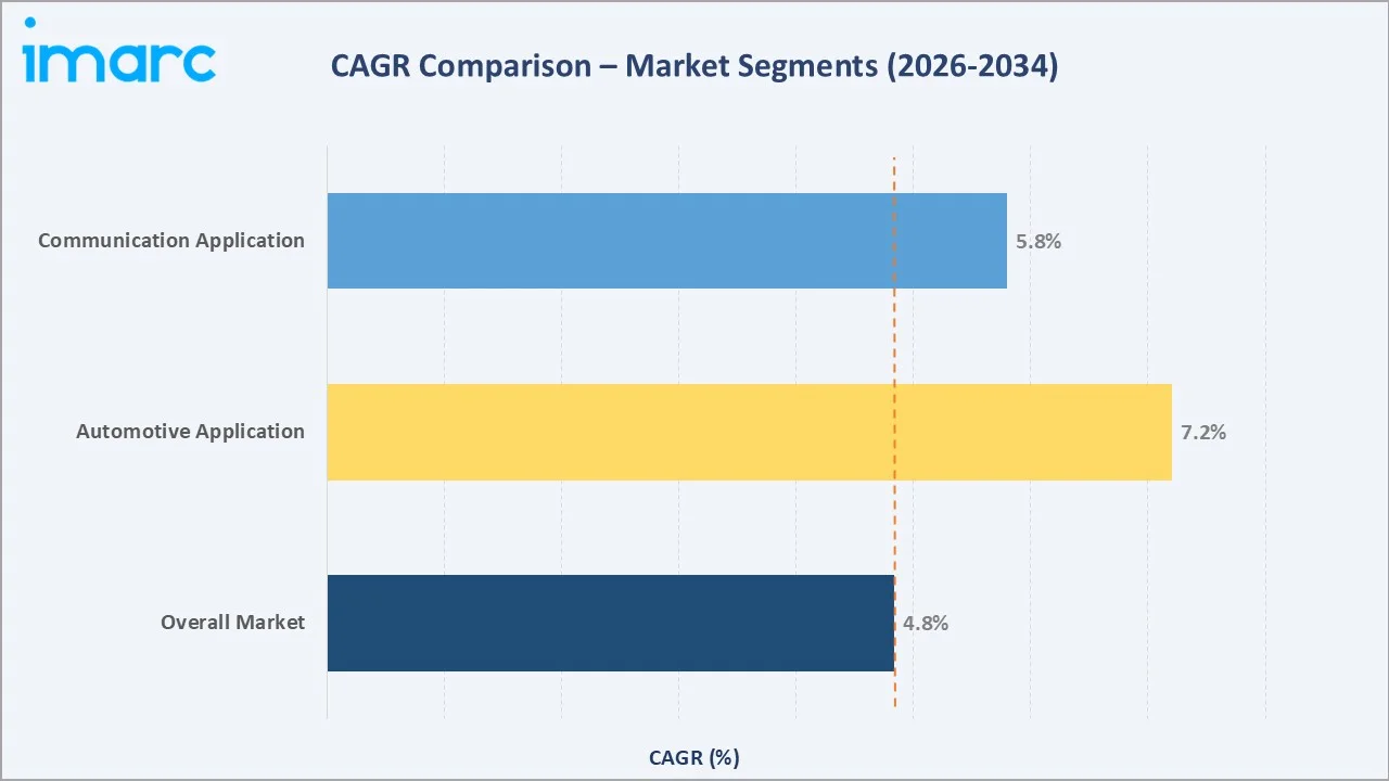
The automotive segment is growing at a 7.2% CAGR, and is the fastest-growing application, fueled by ADAS, EV power electronics, and vehicle connectivity chipsets. The overall market CAGR is 4.83%, reflecting increasing fabless design model adoption globally through 2034.
Executive Summary
The global semiconductor foundry market is at the epicenter of the most consequential industrial policy transformation in a generation. From USD 72.06 Billion in 2020, the market grew to USD 91.20 Billion by 2025 through AI chip demand acceleration, 5G infrastructure build-out, and automotive electrification driving record wafer starts. The forecast to USD 141.40 Billion by 2034 reflects a structural re-ordering of semiconductor manufacturing geography, driven by USD 250+ Billion in announced government incentives globally, including the U.S. CHIPS Act, the EU Chips Act, Japan’s semiconductor strategy, and India’s India Semiconductor Mission.
IDMs retain dominance at 63.7% market share (2025), encompassing Samsung’s integrated IDM/foundry model, Intel’s Foundry Services transformation, and specialty IDMs (STMicroelectronics, Infineon, Renesas) with internal wafer fabrication. Pure play foundries at 36.3% are growing at the faster ~6.4% CAGR, led by TSMC’s unmatched advanced node process leadership.
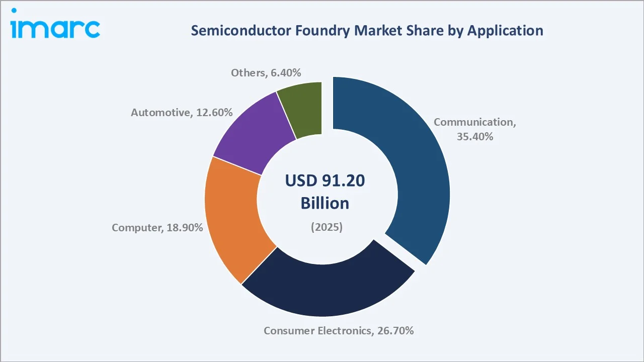
The communication application segment dominates at 35.4%, driven by 5G modems, millimeter wave antenna ICs, and satellite communication chip demand. Automotive at 12.6% is the fastest growing application segment at ~7.2% CAGR, fueled by EV power electronics, ADAS radar, and in-vehicle infotainment semiconductors.
Asia Pacific’s commanding 71.2% regional share (2025) reflects Taiwan’s TSMC monopoly on advanced nodes, South Korea’s Samsung capacity, and China’s rapidly expanding domestic foundry ecosystem despite export control constraints. However, North America is the fastest-growing region at approximately 7.2% CAGR through 2034, as the CHIPS Act allocated $53 Billion to support semiconductor manufacturing and research and development, along with offering a 25% refundable tax credit on eligible capital expenditures.
Key Market Insights
|
Insight |
Data |
|
Dominant Foundry Type |
IDMs - 63.7% revenue share (2025) |
|
Largest Application |
Communication - 35.4% revenue share (2025) |
|
Leading Region |
Asia Pacific - 71.2% revenue share (2025) |
|
Fastest Growing Region |
North America (CAGR ~7.2%, 2026-2034) |
Key Analytical Observations Supporting The Above Data:
- IDMs dominate at 63.7% (2025): Samsung Electronics and SK Hynix together manufacture approximately 60% of the world’s NAND flash, with its foundry services segment adding external wafer revenues.
- Communication leads at 35.4% (2025): Over 1 Billion 5G subscriptions are expected by 2031, reaching 79% subscription penetration, each requiring 4–6 advanced node chips for modem, RF transceiver, and application processor functions.
- Asia Pacific holds 71.2% share (2025): Taiwan’s advanced node global foundry capacity is driving the market growth. This extraordinary geographic concentration is the primary driver of the global government investment to diversify foundry capacity to the U.S., Europe, Japan, and India, a diversification effort that represents the foundry market’s most significant structural change.
- North America's fastest-growing region at ~7.2% CAGR: TSMC’s first Arizona fabrication plant, producing chips using N4 process technology in 2024, began building a second facility, which is expected to commence 3nm production in 2026, representing a combined investment.
Global Semiconductor Foundry Market Overview
A semiconductor foundry, also called a semiconductor fabrication plant or fab, is a manufacturing facility that produces integrated circuits on silicon wafers for external customers (fabless design companies and IDMs outsourcing overflow capacity). The foundry model, pioneered by TSMC in 1987, enables specialization: fabless design companies focus on IC design without owning expensive manufacturing infrastructure, while pure-play foundries concentrate on process technology innovation and manufacturing efficiency.
The foundry ecosystem serves five primary application verticals: communication (5G devices, networking ICs), consumer electronics (smartphones, TVs, wearables), computers (CPUs, GPUs, AI accelerators, memory), automotive (ADAS, EV power electronics, infotainment), and industrial/other (IoT, medical, defense).
Macroeconomic drivers include global semiconductor demand, the AI infrastructure investment cycle, and geopolitical realignment of supply chains under the U.S. Export Administration Regulations (EAR) restricting advanced semiconductor equipment exports.
Market Dynamics
To evaluate market opportunities, Request Sample
Market Drivers
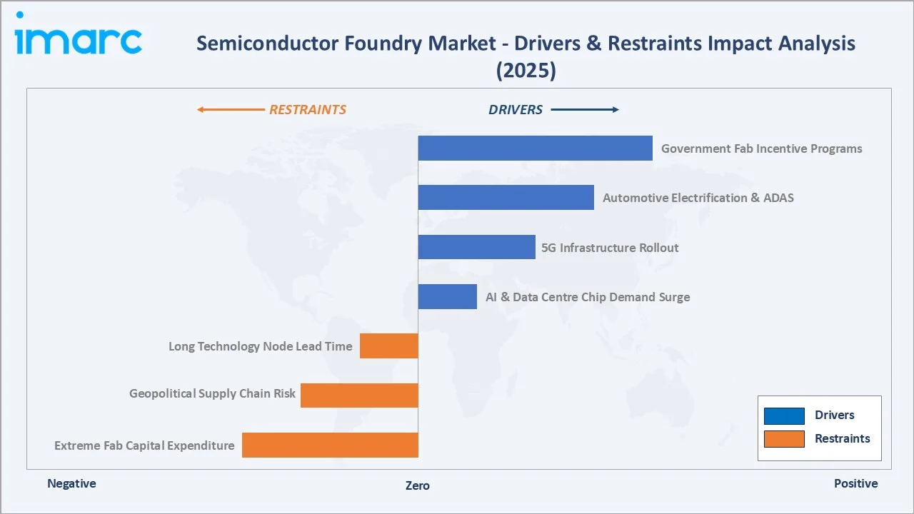
- AI and HPC Silicon Demand Surge: AI accelerator silicon demand has driven advanced packaging capacity to 100% utilization, with customer waiting lists extending 18–24 months for advanced packaging allocations.
- 5G Network Infrastructure and Device Rollout: Global 5G connections reached 2.7 Billion in 2025 and are projected to reach 5.5 Billion by 2030. Each 5G base station requires 3–5× more semiconductor content than 4G, with RF front-end modules, baseband processors, and power amplifiers all manufactured at advanced foundry nodes.
- Automotive Electrification and ADAS: Global electric car sales reached 17 million units in 2024, requiring power semiconductors, ADAS chips, and infotainment SoCs in unprecedented volumes.
- Government Subsidies Reshaping Fab Investment Economics: The US CHIPS and Science Act committed USD 52.7 Billion for domestic semiconductor manufacturing. These subsidies reduce effective fab investment cost, enabling geographic diversification of foundry capacity.
Market Restraints
- Extreme Capital Intensity of New Fabs: A single greenfield 300mm wafer fab at an advanced node requires high capital investment and 5–7 years from groundbreaking to production-ready capacity.
- Semiconductor Talent Shortage: The U.S. semiconductor industry faces a shortage of approximately 67,000 engineers and technicians by 2030, with the EU and Japan reporting comparable workforce gaps.
Market Opportunities
- Advanced Packaging as a New Foundry Revenue Category: Chip-on-Wafer-on-Substrate (CoWoS) and System-on-Integrated-Chip (SoIC) advanced packaging creates a market opportunity.
- Specialty Semiconductor Demand for Automotive and Industrial: Wide-bandgap semiconductor foundry services, including Silicon Carbide (SiC) for EV power modules and Gallium Nitride (GaN) for RF and power conversion, represent a premium-price, high-growth opportunity.
- India’s Semiconductor Manufacturing Emergence: The India Semiconductor Mission invested USD 15 Billion for the second phase of chip manufacturing incentive policy, creating a new geographic node in the global foundry supply chain.
Market Challenges
- ASML EUV Lithography Supply Constraint: ASML’s High-NA EUV systems, required for 2nm and below logic manufacturing, are premium priced with an annual production capacity of approximately 20 systems per year.
- Technology Migration Risk at Sub-2nm Nodes: The industry is at a fundamental inflection point in transistor architecture: the transition from FinFET to Gate-All-Around (GAA) transistors introduces new manufacturing complexity, yield challenges, and design rule changes that require complete redesigns of existing chip products.
Emerging Market Trends
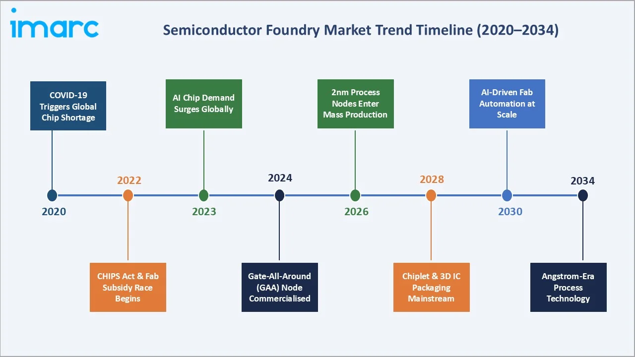
1. Gate-All-Around (GAA) Transistors Replacing FinFET Below 3nm
Gate-All-Around (GAA) nanosheet transistors, the successor to FinFET architecture, provide superior electrostatic control, enabling continued transistor density scaling below 3nm. In June 2022, Samsung Electronics started initial production of its 3nm process node, applying Gate-All-Around (GAA) transistor architecture.
2. Chiplet Architecture and Advanced Packaging Revolution
The end of monolithic SoC scaling driven the industry to heterogeneous chiplet integration: combining multiple smaller dies via advanced packaging technologies.
3. Government-Driven Geographic Diversification
The U.S. CHIPS Act, EU Chips Act, Japan METI strategy, and India Semiconductor Mission collectively represent the largest government intervention in the manufacturing sector location since the Second World War.
4. Sustainability and Low-Carbon Semiconductor Manufacturing
Semiconductor fabrication is highly energy and water-intensive: a typical fab can use up to 30-50 MW of peak electrical capacity. To make 1,000 gallons of UPW, approximately 1,600 gallons of municipal water are needed. This further drives the demand for sustainability and low-carbon semiconductor manufacturing.
Industry Value Chain Analysis
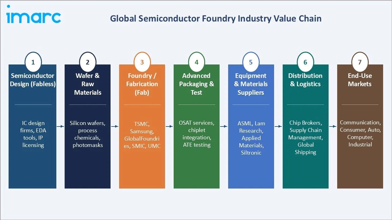
The semiconductor foundry value chain spans from raw material extraction and equipment manufacturing through wafer fabrication, chip packaging, and system assembly to end-use product delivery. Each stage requires extraordinary specialization and capital intensity.
|
Stage |
Key Players & Examples |
|
Raw Materials & Chemicals |
Silicon wafers, photoresists, ultra-high purity gases, CMP slurries |
|
Semiconductor Equipment |
EUV/DUV lithography, etch/deposition, inspection |
|
Foundry Fabrication |
TSMC, Samsung Foundry, Intel Foundry, GlobalFoundries |
|
End-Use Industry Verticals |
Communication OEMs, consumer electronics brands, PC/server makers, auto OEMs, cloud hyperscalers |
Wafer fabrication captures the largest share of total semiconductor value chain revenue. The equipment layer, captures more of the foundry capital expenditure, creating an extraordinary supplier leverage dynamic where ASML’s EUV monopoly gives it pricing power over even the world’s largest chip manufacturers.
Technology Landscape in the Semiconductor Foundry Industry
Advanced Logic Process Nodes: FinFET to GAA Transition
The progression from 5nm FinFET (TSMC N5, 2020) through 3nm FinFET (N3, 2022), 2nm GAA (N2, 2025), represents the cutting edge of semiconductor manufacturing. Each node transition requires new photolithography, new materials, and new transistor architectures.
EUV and High-NA EUV Lithography
Extreme Ultraviolet (EUV) lithography, using 13.5nm wavelength light to print circuit patterns with 5–13nm half-pitch resolution is required for all process nodes below 7nm.
Advanced Packaging: CoWoS, SoIC, and Foveros
Chip-on-Wafer-on-Substrate (CoWoS) known for its best-in-class package technology for ultra-high performance computing applications, such as AI and supercomputing. CoWoS-S supports interposers up to 3.3X-reticle size. For interposers larger than this, CoWoS-L or CoWoS-R are recommended.
Wide-Bandgap Semiconductors (SiC and GaN)
Silicon Carbide (SiC) power devices, with 3× higher breakdown voltage and 10× higher thermal conductivity than silicon, are replacing silicon IGBTs in EV inverters, solar inverters, and industrial motor drives.
Market Segmentation Analysis
The report covers the following segments:
| Segment Category | Leading Segment | Market Share | Year |
|---|---|---|---|
| Technology Node | 10/7/5nm | 36.2% | 2025 |
| Foundry Type | IDMs | 63.7% | 2025 |
| Application | Communication | 35.4% | 2025 |
| Region | Asia Pacific | 71.2% | 2025 |

By Application
To access detailed market analysis, Request Sample
Communication dominates with 35.4% market share (2025). This segment is anchored by 5G modem SoCs, RF front-end modules, application processors for smartphones, and satellite communication chipsets.
Consumer electronics at 26.7% encompasses smartphone SoCs, smart TV chips, wearable ICs, and gaming semiconductor demand. Computer at 18.9% is driven by AI GPU, CPU, and data center accelerator demand, the fastest-growing sub-segment within this category at approximately 22% CAGR. Automotive at 12.6% is growing at ~7.2% CAGR, the fastest application segment through 2034.
By Foundry Type
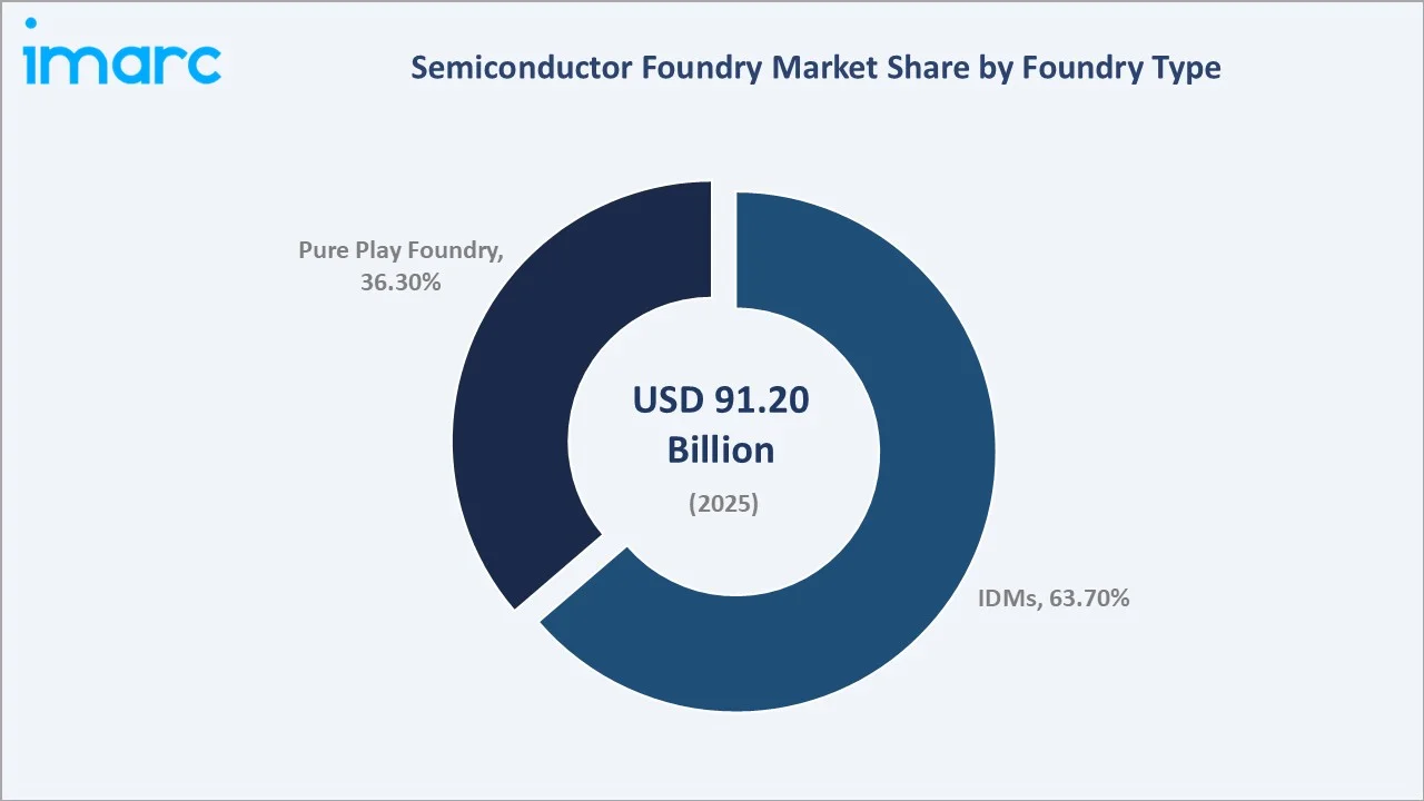
IDMs dominate with 63.7% market share (2025). IDMs benefit from being able to optimize process technology specifically for their proprietary chip designs, a significant advantage that pure-play foundries cannot offer.
Pure play foundries at 36.3% are growing faster at approximately 6.4% CAGR through 2034. The pure-play model’s strategic advantage is that it never competes with its own customers, a critical trust element enabling fabless companies to share their most sensitive next-generation chip designs with their foundry partner.
Regional Market Insights
|
Region |
Share (2025) |
Key Growth Drivers |
|
Asia Pacific |
71.2% |
TSMC Taiwan capacity leadership; Samsung Korea advanced nodes; SMIC China domestic push; India Semiconductor Mission |
|
North America |
12.6% |
U.S. CHIPS Act; Intel Ohio Fab (IFS); GlobalFoundries NY expansion |
|
Europe |
9.8% |
EU Chips Act; TSMC Dresden fab; Intel Magdeburg fab |
|
Latin America |
3.5% |
Brazil semiconductor packaging assembly growth; Mexico nearshoring electronics; Chile critical minerals for semiconductor supply chains |
|
Middle East & Africa |
2.9% |
UAE hub for semiconductor design (Alif Semiconductor); Saudi Arabia Vision 2030 tech diversification |
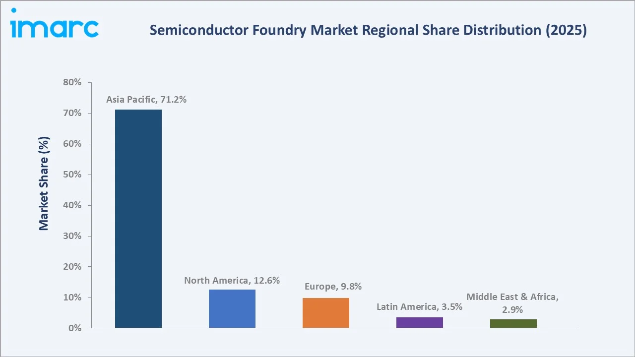
Asia Pacific’s extraordinary 71.2% market dominance (2025). Taiwan, a critical hub in the global semiconductor supply chain, accounting for over 60% of global foundry revenue and over 90% of leading-edge chip manufacturing. The India Semiconductor Mission invested USD 15 Billion for the second phase of chip manufacturing incentive policy.
North America at 12.6% (2025), at ~7.2% CAGR, is the fastest growing regional share in the global foundry market. Europe at 9.8% (2025) is being fundamentally reshaped by the EUR 43 Billion EU Chips Act. European foundries benefit from structural demand for automotive-grade chips manufactured within European supply chains for EU OEM customers.
Competitive Landscape
The global semiconductor foundry market is highly concentrated at the technology frontier and moderately fragmented across mature process nodes. TSMC alone accounts for approximately 57–60% of total pure-play foundry revenue. The top three players, TSMC, Samsung Foundry, and Intel Foundry, collectively control over 90% of sub-5nm advanced logic production capacity globally.
|
Company Name |
Key Products / Services |
Market Position |
Core Strength |
|
Taiwan Semiconductor Manufacturing Company Limited (TSMC) |
12-inch FABs, 8-inch Fabs, Advanced Backend Fabs |
Market Leader |
World’s largest pure-play foundry, dominance in sub-3nm production |
|
Samsung |
Samsung Foundry (14/10/8/5/4nm FinFet, and 3nm GAA with EUV technology from 7nm, Samsung Foundry’s SAFE) |
Market Leader |
Only competitor to TSMC at advanced nodes (3nm GAA), integrated IDM model with own product volume |
|
Intel Corporation |
Intel 18A, Intel 3: Intel’s Ultimate FinFET Node, Intel 16, Intel 14A, and 2D, 2.5D, and 3D packaging |
Strong Challenger |
Transitioning to the foundry model, Intel 18A (1.8nm) targets external customers, the U.S. government CHIPS Act beneficiary |
|
GlobalFoundries |
Wafer services, Module services, Engineering services |
Strong Challenger |
World’s largest specialty foundry, CHIPS Act recipient |
|
DB HiTek |
BCDMOS, Analog CMOS, CIS, MS/RF, SJ MOSFET, SiC, GaN |
Specialist |
Korea’s specialty analog foundry; power management IC (PMIC) and display driver IC (DDI) leadership |
|
Hua Hong Semiconductor Ltd. |
Embedded Memory, Standalone Memory, Power Discrete Devices, Logic and RF Platform |
Established |
China’s second-largest foundry; specialty in power devices |
|
Powerchip Semiconductor Manufacturing Corporation |
8-inch wafer fabs, 12-inch wafer fabs |
Established |
Taiwan foundry for DRAM and logic, niche OLED driver IC and power management foundry services |
The technology-driven concentration is structurally different from most industries and reflects the fundamental reality that only organizations capable of USD 30–40 Billion annual capital investment can remain at the leading edge.
Key Company Profiles
Taiwan Semiconductor Manufacturing Company Limited (TSMC)
TSMC is the world’s largest dedicated semiconductor foundry and the most critical company in the global technology supply chain. TSMC’s N2 (2nm GAA) process, entering volume production in late 2025, represents the world’s most advanced manufacturing technology available to external customers.
- Product Portfolio: N2 GAA (2nm), N3 (3nm FinFET), N4P (4nm), N5 (5nm FinFET), CoWoS and SoIC advanced packaging.
- Recent Developments: In April 2026, TSMC is expected to launch equipment installation and mass production of 3-nanometre wafers in 2028 at its second factory in Japan.
- Strategic Focus: Maintaining 2nm/1.4nm technology leadership; geographic diversification; CoWoS capacity tripling by 2026 for AI GPU demand; High-NA EUV ramp for N14 below-1.4nm development; U.S. and EU government strategic partnership deepening.
Samsung
Samsung is the world’s largest IDM and TSMC’s only competitor at the most advanced logic process nodes, with its foundry business. The Samsung Foundry division, combined with its internal semiconductor divisions (DRAM, NAND, system LSI), positions Samsung as the only vertically integrated semiconductor company capable of designing, manufacturing, and packaging the full range of chips.
- Product Portfolio: 28FD-SOI, 14/10/8/5/4nm FinFet, and 3nm GAA with EUV technology from 5nm, Samsung Foundry’s SAFE.
- Recent Developments: In June 2024, Samsung unveiled its latest foundry innovations and outlined its vision for the AI era during Samsung Foundry Forum (SFF) U.S.
- Strategic Focus: GAA transistor yield recovery to match TSMC competitiveness; U.S. fab completion for CHIPS Act incentives and Qualcomm/Google Tensor ASIC recapture; HBM4 memory integration with advanced packaging for AI GPU competition.
GlobalFoundries
GlobalFoundries is one of the world’s largest pure-play foundries by revenue, focusing exclusively on specialty and differentiated process technologies at mature nodes where it faces less direct competition from TSMC and Samsung.
- Product Portfolio: Wafer services, Module services, Engineering services.
- Recent Developments: In November 2025, GlobalFoundries acquired Advanced Micro Foundry (AMF), marking a pivotal step in GF’s strategy to advance innovation and its leadership in silicon photonics.
- Strategic Focus: Specialty process differentiation where TSMC and Samsung are not competitive; automotive and IoT long-term supply agreements providing revenue predictability; CHIPS Act-enabled U.S. capacity expansion; defense and aerospace secure fabrication under DOD Trusted Foundry program.
Intel Corporation
Intel is executing its most significant strategic transformation since the Intel Architecture transition, re-positioning from a captive IDM to an open foundry accepting external customers through Intel Foundry.
- Product Portfolio: Intel 18A, Intel 3: Intel’s Ultimate FinFET Node, Intel 16, Intel 14A and Intel 14A-E, 2D, 2.5D, and 3D packaging.
- Recent Developments: In February 2024, Intel launched its contract chip manufacturing business to compete against Asian foundry giants TSMC and Samsung, known as “world’s first systems foundry” for the AI era and disclosing its next-generation Intel 14A process node that is expected to arrive in 2026.
- Strategic Focus: Intel 18A external customer ramp as IDM-to-foundry pivot proof point; Foveros advanced packaging as unique competitive differentiator; U.S. government defense chip fabrication under CHIPS Act requirements; regaining internal process leadership versus TSMC by 2027 per Intel Accelerated roadmap.
Market Concentration Analysis
The semiconductor foundry market exhibits extreme concentration at the leading-edge technology tier and moderate fragmentation at mature process nodes. TSMC alone accounts for approximately 55–58% of total pure-play foundry revenue globally, a concentration ratio that has no parallel in any other major technology manufacturing sector.
The top players, TSMC, Samsung Foundry, Intel Foundry, GlobalFoundries, collectively account for approximately 75–78% of total foundry market revenue, placing the industry firmly in the oligopolistic concentration zone. Consolidation at the leading edge is effectively complete, while specialty node consolidation is accelerating.
Investment & Growth Opportunities
Fastest Growing Segments
Automotive chips (CAGR ~7.2%), AI/HPC computer chips (CAGR ~15%+ for AI accelerators), and advanced packaging (CAGR ~25%) represent the three highest-return investment vectors within the semiconductor foundry market through 2034. SiC and GaN wide-bandgap foundry services, growing at approximately 32% CAGR through 2028, represent the most attractive niche opportunity for specialty foundries willing to invest in non-silicon process capability.
Emerging Market Opportunities
India’s first major semiconductor fabs, Tata/PSMC and potentially ISMC, represent the first significant greenfield foundry investments in the subcontinent. India’s 1.4 Billion population creates structural demand for domestically manufactured chips for smartphones, EVs, and government digital programs (Aadhaar, UPI, DigiYatra) that currently consume imported semiconductors annually.
Venture Investment Trends
Government-backed investment vehicles, including the CHIPS Act Direct Funding Program, EU Important Projects of Common European Interest (IPCEI), and Japan’s LSTC (Leading-edge Semiconductor Technology Center), are functioning as de facto late-stage venture capital for advanced foundry expansion.
- Strategic focus: AI accelerator chip architectures (custom ASICs replacing GPUs), chiplet standardization (UCIe ecosystem companies), EUV mask and equipment companies, and advanced packaging substrate manufacturers.
- Private equity: PE interest in second-tier specialty foundries targeting bolt-on acquisitions to build diversified automotive and analog specialty foundry platforms across U.S., Europe, and Japan geographies.
Future Market Outlook (2026-2034)
The global semiconductor foundry market is set for sustained, structurally supported growth from USD 91.20 Billion in 2025 to USD 141.40 Billion by 2034. This USD 50.2 Billion absolute addition over nine years at 4.83% CAGR masks dramatically divergent trajectories within the market. Advanced node (sub-5nm) foundry revenue will grow at approximately 15–18% CAGR driven by AI accelerator demand, while mature node (28nm+) foundry revenue grows at 2–3% as capacity expansion from government-incentivized fabs adds supply. Advanced packaging is the fastest-growing category at 25%+ CAGR, becoming foundry revenue’s second largest contributor by 2028.
Between 2026 and 2030, the dominant transformation will be the geographic diversification of advanced node capacity as TSMC Arizona N3/N2, Intel Ohio 18A, and Samsung Taylor fabs enter production. More significantly, it will create a high annual foundry market outside Asia Pacific for the first time, enabling U.S. and EU defense programs, cloud hyperscalers, and automotive OEMs to source mission-critical chips domestically.
Research Methodology
Primary Research
Primary research for this report included structured interviews with 140+ industry stakeholders in 2025, comprising foundry executives, fabless IC design company procurement officers, semiconductor equipment company analysts, government officials administering CHIPS Act and EU Chips Act programs, and equity research analysts specializing in semiconductor technology. Geographic coverage included Taiwan, South Korea, Japan, the U.S., Germany, the Netherlands, and India.
Secondary Research
Secondary research encompassed SEMI equipment and materials market reports, SIA global semiconductor sales data, IC Insights foundry market reports, company annual reports and earnings transcripts, government CHIPS Act application disclosures, patent filing databases, NIST semiconductor roadmaps, and IEDM/ISSCC academic conference proceedings. Over 290 secondary sources were reviewed and cross-referenced.
Forecasting Models
Market size forecasts were developed using a combination of bottom-up and top-down methodologies. Key inputs include ASML EUV delivery schedules, government fab investment commitment timelines, AI accelerator demand projections, and automotive semiconductor content per vehicle growth curves. Three-scenario modelling was applied across the 2026–2034 forecast horizon.
Semiconductor Foundry Market Report Scope:
| Report Features | Details |
|---|---|
| Base Year of the Analysis | 2025 |
| Historical Period | 2020-2025 |
| Forecast Period | 2026-2034 |
| Units | Billion USD |
| Scope of the Report | Exploration of Historical Trends and Market Outlook, Industry Catalysts and Challenges, Segment-Wise Historical and Future Market Assessment:
|
| Technology Nodes Covered | 10/7/5nm, 16/14nm, 20nm, 45/40nm, Others |
| Foundry Types Covered | Pure Play Foundry, IDMs |
| Applications Covered | Communication, Consumer Electronics, Computer, Automotive, Others |
| Regions Covered | Asia Pacific, Europe, North America, Latin America, Middle East and Africa |
| Countries Covered | United States, Canada, Germany, France, United Kingdom, Italy, Spain, Russia, China, Japan, India, South Korea, Australia, Indonesia, Brazil, Mexico |
| Companies Covered | Taiwan Semiconductor Manufacturing Company Limited (TSMC), Samsung, Intel Corporation, GlobalFoundries, DB HiTek, Hua Hong Semiconductor Ltd., Powerchip Semiconductor Manufacturing Corporation, etc. |
| Customization Scope | 10% Free Customization |
| Post-Sale Analyst Support | 10-12 Weeks |
| Delivery Format | PDF and Excel through Email (We can also provide the editable version of the report in PPT/Word format on special request) |
Key Benefits for Stakeholders:
- IMARC’s report offers a comprehensive quantitative analysis of various market segments, historical and current market trends, market forecasts, and dynamics of the semiconductor foundry market from 2020-2034.
- The semiconductor foundry market research report provides the latest information on the market drivers, challenges, and opportunities in the global market.
- The study maps the leading, as well as the fastest-growing, regional markets. It further enables stakeholders to identify the key country-level markets within each region.
- Porter's five forces analysis assist stakeholders in assessing the impact of new entrants, competitive rivalry, supplier power, buyer power, and the threat of substitution. It helps stakeholders to analyze the level of competition within the semiconductor foundry industry and its attractiveness.
- Competitive landscape allows stakeholders to understand their competitive environment and provides an insight into the current positions of key players in the market.
Frequently Asked Questions About the Semiconductor Foundry Market Report
The global semiconductor foundry market was valued at USD 91.20 Billion in 2025 and is projected to reach USD 141.40 Billion by 2034, growing at a CAGR of 4.83%.
Asia Pacific dominates with 71.2% revenue share (2025), anchored by TSMC Taiwan, Samsung Korea, and China’s SMIC domestic foundry expansion.
IDMs lead with 63.7% market share (2025). Samsung Electronics, Intel, and specialty IDMs collectively fabricate the majority of global semiconductor volume internally alongside offering external foundry services.
Communication leads with 35.4% share (2025), driven by 5G modem chips, RF front-end modules, and application processors for smartphones manufactured at TSMC’s most advanced process nodes.
The top market players include Taiwan Semiconductor Manufacturing Company Limited (TSMC), Samsung, Intel Corporation, GlobalFoundries, DB HiTek, Hua Hong Semiconductor Ltd., and Powerchip Semiconductor Manufacturing Corporation.
Key trends include GAA transistor adoption below 3nm, chiplet and advanced packaging growth, government-driven fab geographic diversification, SiC/GaN wide-bandgap specialty foundries, and silicon photonics for AI interconnects.
The USD 52.7B CHIPS Act is catalyzing TSMC Arizona (N2 by 2028), Intel Ohio (18A by 2027), GlobalFoundries Malta expansion, and Micron Idaho, adding U.S. fab investment through 2030.
Extreme capital requirements, ASML EUV monopoly, 5–7 year fab build timelines, and decades of cumulative process R&D create insurmountable barriers to entry at advanced nodes.
Automotive is the fastest growing application at ~7.2% CAGR, driven by EV power electronics, ADAS chips, and infotainment SoCs with semiconductor content per vehicle.
Key challenges include fab capital intensity, ASML High-NA EUV supply constraints (20 units/year), geopolitical export controls restricting SMIC’s advanced node access, and structural semiconductor talent shortages.
Top opportunities include AI accelerator advanced packaging (CoWoS/SoIC), SiC/GaN automotive foundry, North America CHIPS Act-beneficiary foundries, India’s first semiconductor fabs, and chiplet integration ecosystem companies.
Need more help?
- Speak to our experienced analysts for insights on the current market scenarios.
- Include additional segments and countries to customize the report as per your requirement.
- Gain an unparalleled competitive advantage in your domain by understanding how to utilize the report and positively impacting your operations and revenue.
- For further assistance, please connect with our analysts.
 Request Customization
 Speak to an Analyst
 Request Brochure
 Inquire Before Buying
Benefits of Customization
- Personalize this research
- Triangulate with your data
- Get data as per your format and definition
- Gain a deeper dive into a specific application, geography, customer, or competitor
- Any level of personalization
Get in Touch With Us
UNITED STATES
Phone: +1-201-971-6302
INDIA
Phone: +91-120-433-0800
UNITED KINGDOM
Phone: +44-753-714-6104
Email: [email protected]
Client Testimonials



.webp)



.webp)








Related Reports

Choose your plan
*Please note that the prices mentioned below are starting prices for each bundle type. Kindly contact our team for further details.*
Single User License
- 1 User License, Access on 2 Devices
- PDF Report + Excel Dataset (Password Protected)
- Lifetime Access
- No Printing Rights
- 10% Free Report Customization
- 10–12 Weeks of Analyst Support
Five User License
- Access for 5 Users, 2 Devices per User
- PDF Report + Excel Dataset (Password Protected)
- Lifetime Access
- Dedicated Account Manager
- 12–14 Weeks of Analyst Support
- No Printing Rights
- 15% Free Report Customization
- 25% Discount on Your Next Purchase
Corporate User License
- Unlimited User Access (Within Your Organization)
- PDF Report + Excel Dataset
- Lifetime Access
- Dedicated Account Manager
- 14–20 Weeks of Analyst Support
- No Printing Rights
- 20% Free Report Customization
- 30% Discount on Your Next Purchase
Essential Insights
What's included:
3 reports
- Lifetime Access
- PDF Reports
- Excel Datasets
- 2 Weeks of Free Analyst Support
- 2 User Licenses
- Access on 2 Devices
- Printing Rights
- Complimentary PowerPoint (PPT) Version
- Complimentary License Upgrade
Professional Access
What's included:
5 reports
- Lifetime Access
- PDF Reports
- Excel Datasets
- 8 Weeks of Free Analyst Support
- 2 User Licenses
- Access on 2 Devices
- Printing Rights
- Complimentary PowerPoint (PPT) Version
- Complimentary License Upgrade
Business Advantage
What's included:
8 reports
- Lifetime Access
- PDF Reports
- Excel Datasets
- 14 Weeks of Free Analyst Support
- 2 User Licenses
- Access on 2 Devices
- Printing Rights
- Complimentary PowerPoint (PPT) Version
- Complimentary License Upgrade
Enterprise Intelligence
What's included:
10 reports
- Lifetime Access
- PDF Reports
- Excel Datasets
- 20 Weeks of Free Analyst Support
- 2 User Licenses
- Access on 2 Devices
- Printing Rights
- Complimentary PowerPoint (PPT) Version
- Complimentary License Upgrade