Silicon Wafer Market Size, Share, Trends and Forecast by Wafer Size, Type, Application, End Use, and Region, 2026-2034
Global Silicon Wafer Market Size, Share, Trends & Forecast (2026-2034)
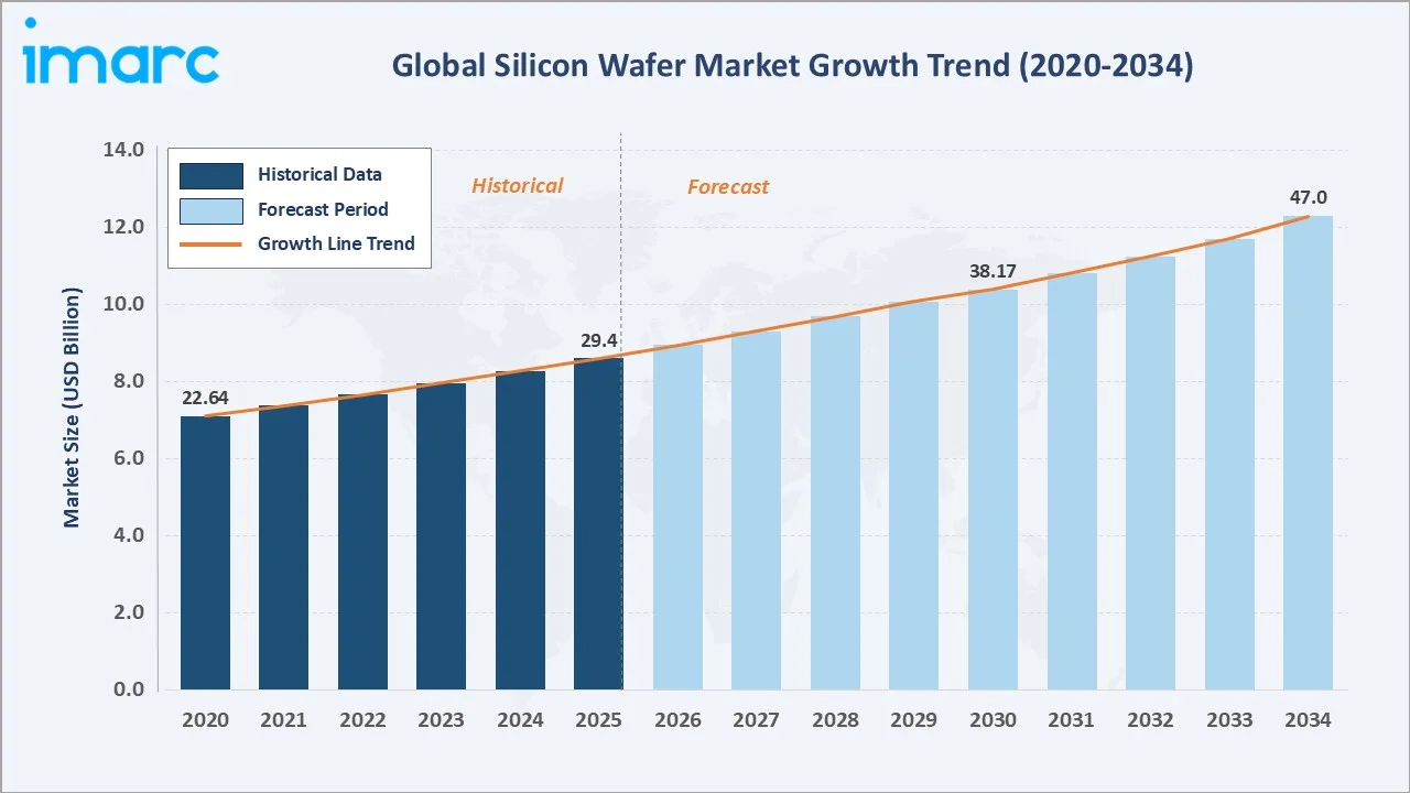
The global silicon wafer market size was valued at USD 29.4 Billion in 2025 and is projected to reach USD 47.0 Billion by 2034, expanding at a robust CAGR of 5.36% during the forecast period 2026-2034. The market's strong growth trajectory is driven by exponential demand for semiconductor devices across AI & high-performance computing and massive government-backed fab investment programs such as the US CHIPS & Science Act and EU Chips Act.
Market Snapshot
|
Report Attribute |
Key Statistics |
|
Market Size in 2025 |
USD 29.4 Billion |
|
Market Forecast in 2034 |
USD 47.0 Billion |
|
Base Year |
2025 |
|
Forecast Years |
2026-2034 |
|
Market Growth Rate (2026-2034) |
5.36% CAGR |
|
Largest Region (2025) |
Asia Pacific - 68.5% |
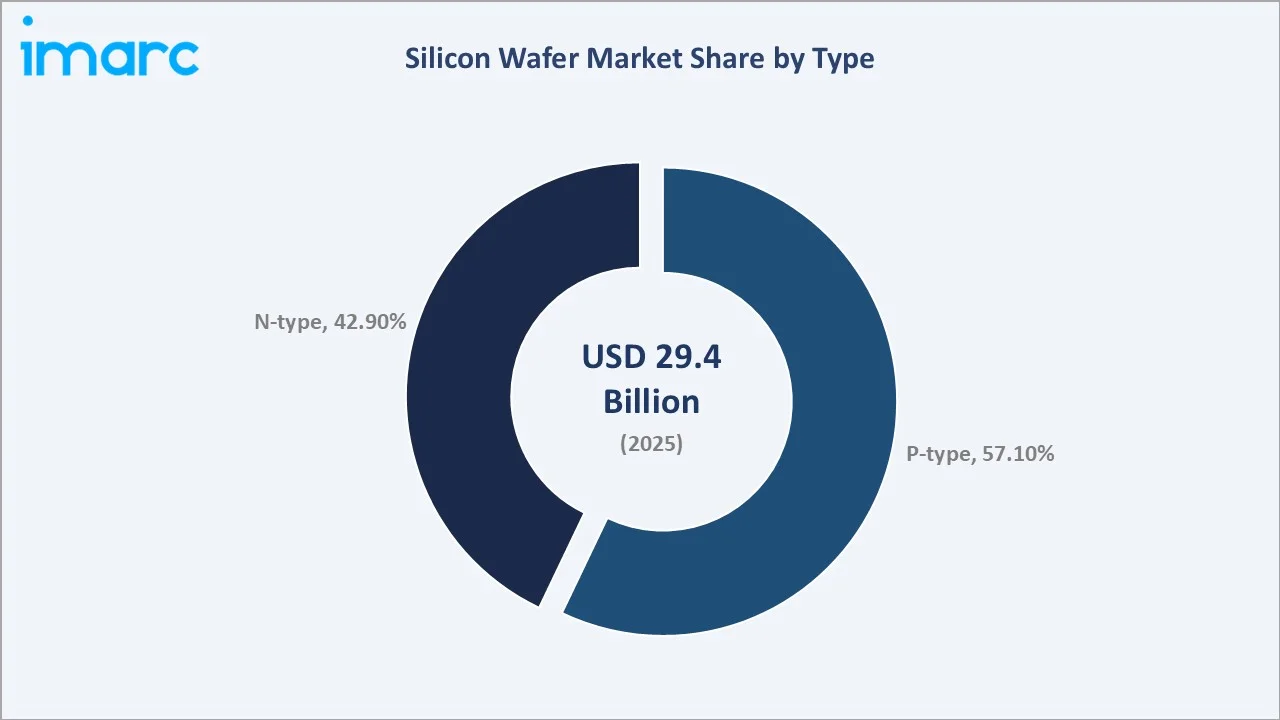
Asia Pacific dominates the global market, accounting for 68.5% of revenue in 2025, anchored by the concentrated presence of the world’s leading semiconductor fabs and wafer manufacturers across Japan, South Korea, Taiwan, and China. Among wafer types, P-type wafers command the largest share at 57.1%, while integrated circuits represent the dominant application at 50.1%.
To get more information on this market, Request Sample
The silicon wafer market forms the foundation of modern electronics manufacturing, serving as the essential substrate for semiconductor device fabrication. Its growth is closely tied to advancements in digitalization, cloud computing, and high-performance computing applications.
Executive Summary
The global silicon wafer market is experiencing a technology-driven supercycle, underpinned by the convergence of artificial intelligence hardware scaling, 5G deployment, electric vehicle electrification, and unprecedented government investment in sovereign semiconductor manufacturing capacity. Valued at USD 29.4 Billion in 2025, the market is forecast to reach USD 47.0 Billion by 2034 at a CAGR of 5.36%.
Cerebras Systems' Wafer Scale Engine 3 (WSE-3), launched in March 2024 with four trillion transistors on a single 300mm wafer using TSMC's 5nm process, exemplifies the frontier of silicon wafer utilization in AI hardware. The silicon wafer market outlook is further strengthened by the N-type panels, which can reach efficiencies of approximately 42.9%, whereas p-type panels generally peak at around 57.1%.
Asia Pacific's 68.5% market share reflects the deeply entrenched geographic concentration of global semiconductor manufacturing in the region. Japan's Shin-Etsu Chemical and SUMCO alone supply over 50% of the global 300mm wafer volume, investing jointly approximately USD 1 billion in 2025. However, the geopolitical landscape is actively reshaping this concentration, with government-subsidized wafer capacity in the U.S. and Europe diversifying the supply geography meaningfully through the forecast period.
Key Market Insights
|
Insight |
Data |
|
Largest Segment (Type) |
P-type Wafers - 57.1% share (2025) |
|
Largest Segment (Application) |
Integrated Circuits - 50.1% share (2025) |
|
Leading Region |
Asia Pacific - 68.5% revenue share (2025) |
|
Top Companies |
Shin-Etsu Chemical, SUMCO, GlobalWafers, Siltronic, SK Siltron |
|
Key Market Opportunity |
AI & HPC wafer demand by 2034 |
Key Analytical Observations Supporting the Above Data:
- P-type wafers lead with a 57.1% market share (2025) due to their entrenched position in CMOS logic, DRAM, NAND flash, and analog semiconductor manufacturing.
- Integrated circuits dominate applications at 50.1% (2025), encompassing logic processors, memory chips, AI accelerators, and power semiconductors for consumer electronics, data centers, automotive, and telecommunications.
- Asia Pacific's 68.5% dominance reflects the geographic concentration of TSMC, Samsung, and China's expanding domestic fab ecosystem, supported by a dense cluster of wafer manufacturers in Japan, South Korea, and Taiwan.
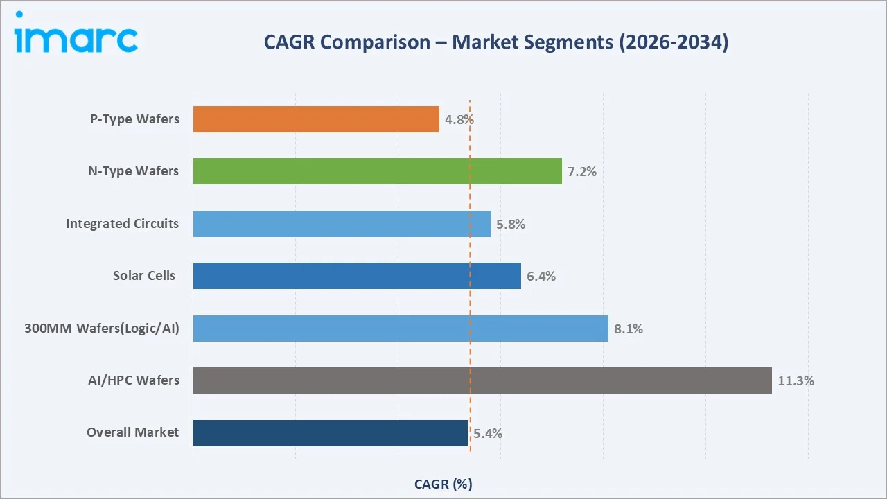
- The AI and HPC segment represents the fastest-growing end-use for premium 300mm silicon wafers, growing at an estimated 11.3% CAGR through 2034.
- Government investment programs, including the US CHIPS Act (USD 52.7 Billion), EU Chips Act (EUR 43 Billion), and India's INR 91,000 crore semiconductor initiative, are collectively creating the largest government-backed silicon wafer demand wave in semiconductor industry history through 2034.
Global Silicon Wafer Market Overview
The silicon wafer industry forms the absolute physical and technological foundation of the global semiconductor economy. Every integrated circuit, from the smallest microcontroller to NVIDIA's multi-trillion-transistor AI accelerator, begins life as a precisely grown, ultra-polished silicon wafer.
Silicon wafers are manufactured through a multi-stage process beginning with the reduction of high-purity quartz sand into polysilicon of 99.99% purity, grown into single-crystal silicon ingots via the Czochralski (CZ) or Float Zone (FZ) process, sliced into wafers, lapped, etched, and polished to atomic-level flatness specifications measured in nanometers.
The silicon wafer market trends through 2034 include the transition to gate-all-around (GAA) transistor architectures at 2nm nodes, the commercialization of SiC and GaN compound semiconductors for power electronics, and the emergence of silicon photonics for data center interconnects - all opening new frontiers of silicon wafer demand that were not present in previous industry cycles.
Market Dynamics
To evaluate market opportunities, Request Sample
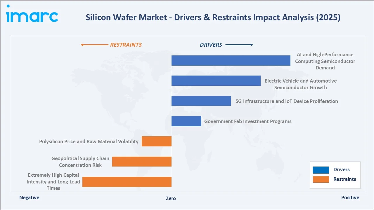
Market Drivers
- AI and High-Performance Computing Semiconductor Demand: NVIDIA's H100 and H200 GPU series, AMD's Instinct accelerators, and hyperscaler custom silicon from Google, Amazon, and Microsoft are collectively growing wafer demand at double-digit rates annually.
- Electric Vehicle and Automotive Semiconductor Growth: More than 1 million additional electric cars were sold in the first quarter of 2025 compared to the same period in 2024, with roughly 60% of these sales occurring in China.
- 5G Infrastructure and IoT Device Proliferation: Global 5G subscriptions are projected to reach 6.4 billion by 2031, driving massive demand for RF front-end modules, millimeter-wave base station chips, and IoT connectivity semiconductors.
- Government Fab Investment Programs: The US CHIPS & Science Act, EU Chips Act, Japan's METI semiconductor support programs, and India's first commercial semiconductor fab are collectively funding new fabrication facilities globally through 2030.
These drivers collectively form the strongest demand environment for silicon wafers in the industry's 70-year history, with multiple simultaneous secular growth catalysts creating a diversified and structurally durable demand base far less cyclical than historical silicon wafer demand patterns.
Market Restraints
- Extremely High Capital Intensity and Long Lead Times: Building a new 300mm wafer fabrication facility requires USD 3-8 billion in capital investment. This creates significant structural lag between demand signals and new capacity, resulting in cyclical supply-demand imbalances that produce price volatility and customer supply insecurity.
- Geopolitical Supply Chain Concentration Risk: The concentration of advanced wafer manufacturing in East Asia creates significant geopolitical supply chain vulnerability. U.S.-China technology trade restrictions, Taiwan Strait tensions, and Japan-Korea trade disputes have all demonstrated the fragility of hyper-concentrated semiconductor supply chains.
- Polysilicon Price and Raw Material Volatility: Polysilicon prices experienced extreme volatility between 2020 and 2024, driven by supply-demand imbalances in the solar industry. This volatility creates input cost uncertainty for silicon wafer manufacturers, particularly those with lower vertical integration degrees.
Market Opportunities
- N-type Wafer Transition in High-Efficiency Solar: The solar PV industry is undergoing a structural transition from P-type to N-type silicon wafers. This transition is expected to double the addressable market for N-type wafers in solar applications by 2028, as NTOPCon modules offer approximately 2–3% higher efficiency (typically 22–24% compared to around 20–21% for PERC), while requiring only a modest cost premium.
- Advanced Packaging and Silicon Interposer Demand: The chiplet revolution driven by TSMC CoWoS-S, Intel EMIB, and AMD 3D V-Cache technologies is creating a new demand category for ultra-thin silicon wafers used as interposers in advanced packaging substrates.
- SiC and GaN Compound Semiconductor Adjacency: Soitec's SmartSiC technology development represents established silicon wafer players successfully entering adjacent compound semiconductor wafer markets driven by EV power electronics and renewable energy conversion applications.
Market Challenges
- 450mm Wafer Transition Uncertainty: The semiconductor industry's long-anticipated transition to 450mm wafers, which would deliver significant cost-per-chip improvements, has been repeatedly delayed due to prohibitive capital requirements.
- Advanced Node Defect Density Requirements: At 2nm and below, wafer defect density requirements approach single-digit defects per cm2, pushing the boundaries of crystal growth, slicing, and polishing technology. Even single sub-nanometer particles can destroy an advanced node chip during fabrication, demanding extraordinary quality control investments.
- China Export Control Escalation Risk: U.S. export controls on advanced semiconductor manufacturing equipment are restricting China's access to leading-edge wafer manufacturing tools. While creating near-term supply diversification benefits for non-Chinese producers, escalating technology decoupling creates long-term market fragmentation risks for the global silicon wafer industry.
Emerging Market Trends
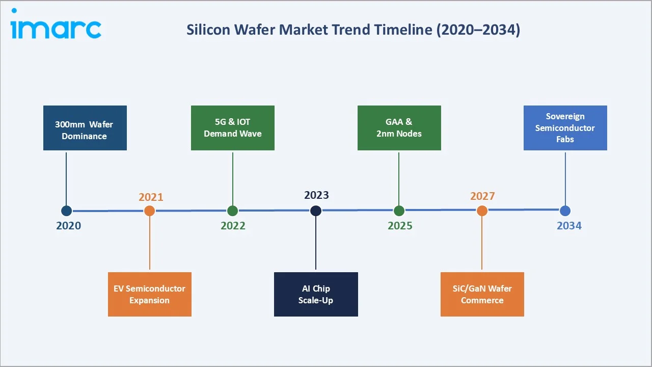
1. 300mm Wafer Dominance and AI-Grade Precision Requirements
The 300mm wafer’s dominance, approximately 68.3% of silicon wafer revenues in 2025, is accelerating as AI chip manufacturing demands unprecedented wafer flatness, purity, and defect control. Shin-Etsu Chemical and SUMCO jointly invested approximately USD 1 billion in 2025 to add ultra-flat 300mm wafer capacity for 2nm and 3nm logic production.
2. N-type Wafer Transition in Solar and Advanced Logic
The N-type silicon wafer revolution is unfolding simultaneously in solar photovoltaics, where the industry-wide migration to TOPCon and HJT architectures is driving N-type demand, and in semiconductor logic, where leading-edge GAA transistor architectures at 3nm and 2nm nodes increasingly favor N-type substrate properties for improved electrostatic control.
3. Sovereign Semiconductor and Domestic Wafer Manufacturing Push
GlobalWafers' USD 5 Billion Sherman, Texas 300mm wafer plant backed by USD 406 Million in CHIPS Act grants targets first wafer production in 2027. On February 27, 2026, Rapidus Corporation announced that it secured a total of 267.6 billion yen in funding, including a 100 billion yen investment from Japan’s Information-Technology Promotion Agency (IPA), as part of a government initiative to ensure stable semiconductor production.
4. SiC and GaN Wafer Commercialization for Power Electronics
Silicon carbide and gallium nitride power semiconductor wafers are experiencing commercial inflection, driven by EV inverters, industrial motor drives, and renewable energy conversion applications. By November 2025, SK Siltron was nearing the final stage of its new plant investment in Gumi, commencing GaN wafer production targeting EV power module manufacturers.
5. Advanced Packaging and Silicon Interposer Demand Growth
The chiplet revolution driven by TSMC CoWoS-S, Intel EMIB, and AMD 3D V-Cache technologies is creating a rapidly growing demand category for ultra-thin silicon wafers used as interposers in 2.5D and 3D-IC package substrates. Silicon interposers are growing at a fast pace as AI chip packaging transitions from monolithic die to chiplet-based architectures.
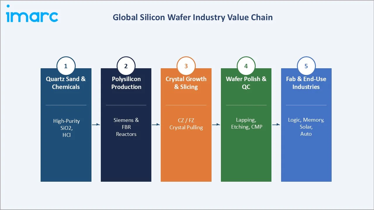
Industry Value Chain Analysis
The silicon wafer value chain is among the most technically demanding and capital-intensive manufacturing sequences in the global industry. Each stage requires precision equipment, ultra-pure materials, and highly controlled cleanroom environments (ISO Class 1-4) to achieve atomic-level quality specifications demanded by modern semiconductor fabs.
|
Stage |
Key Players / Examples |
|
High-Purity Quartz/Fused Silica |
Heraeus Covantics, Sibelco (IOTA), The Quartz Corp., Chlorosilanes/TCS: High-Purity Silicon Corp., HPSA, Tokuyama. |
|
Polysilicon Production |
Wacker, Daqo New Energy, GCL Tech; main processes include Siemens / modified Siemens and FBR granular silicon |
|
Crystal Growth (CZ/FZ) |
Shin-Etsu Chemical, SUMCO, Siltronic, GlobalWafers; Czochralski pullers |
|
Wafer Slicing and Shaping |
Mostly performed in-house by wafer manufacturers using wire-saw technology; historical / equipment example: Meyer Burger. |
|
Lapping, Etching, and Polishing |
In-house at major wafer manufacturers, consumables suppliers include Entegris (CMC Materials legacy) and other CMP-material suppliers. |
|
Epitaxial and SOI Processing |
Soitec (Smart Cut SOI), Shin-Etsu (epi, SOI), Siltronic (epi), GlobalWafers (epi, SOI) |
|
Semiconductor Fabrication |
TSMC, Samsung, Intel Foundry, SMIC, GlobalFoundries, Micron, SK Hynix |
|
End-Use Industries |
Consumer Electronics, Automotive, Industrial, Telecom/Communications, Computing & Data Centers, Memory/Storage |
Asia Pacific's value chain dominance extends from polysilicon production through crystal growth and wafer manufacturing in Japan and South Korea to semiconductor fabrication in Taiwan, South Korea, and China. This geographic compression of the entire supply chain within a single regional cluster provides enormous logistical efficiency advantages but creates systemic concentration risk.
Technology Landscape in the Silicon Wafer Industry
Crystal Growth Technology Innovation
Czochralski (CZ) crystal growth remains the dominant silicon wafer production method. Modern CZ pullers grow 300mm diameter, 2-meter length monocrystalline silicon ingots weighing over 500kg with oxygen concentration controlled at the parts-per-billion level. Magnetic CZ (MCZ), applying magnetic fields to suppress convective turbulence, is increasingly used for memory-grade wafers requiring ultra-low oxygen precipitation.
Advanced Polishing and Surface Preparation
Chemical-mechanical planarization (CMP) for silicon wafer final polishing has advanced to achieve root-mean-square surface roughness below 0.1 nanometers. Next-generation 2nm node wafers require site flatness control (SFQR) below 6 nanometers across any 26mm x 8mm wafer site. Cabot Microelectronics and Fujimi's advanced CMP slurry formulations enable these specifications through precisely engineered nanoparticle chemistry.
Epitaxial Deposition and SOI Wafer Technology
Epitaxial silicon wafer production via chemical vapor deposition is experiencing strong demand growth for logic, power, and image sensor applications. Silicon-on-insulator (SOI) wafers produced via Soitec's Smart Cut technology enable fully depleted SOI transistors with lower power consumption and higher switching speed.
Wafer Inspection and Metrology Technology
Laser surface scanning systems from KLA Corporation and Hitachi High-Technologies detect particles as small as 25nm on 300mm wafer surfaces. Machine learning-enhanced defect classification algorithms are reducing false positive rates by 40-60% compared to rule-based systems, enabling higher production throughput without sacrificing quality escape risk.
Market Segmentation Analysis
The report covers the following segments:
|
Segment Category |
Leading Segment |
Market Share |
Year |
|
Waffer Size |
300mm |
68.3% |
2025 |
|
Type |
P-type |
57.1% |
2025 |
|
Application |
Integrated Circuits |
50.1% |
2025 |
|
End Use |
Solar |
42.1% |
2025 |
|
Region |
Asia Pacific |
68.5% |
2025 |

By Type
To access detailed market analysis, Request Sample
P-type silicon wafers dominate the silicon wafer market with a 57.1% share in 2025, reflecting their entrenched position across CMOS semiconductor manufacturing. P-type wafers doped with boron have been the industry standard substrate for DRAM, NAND flash, analog, and mixed-signal ICs for over four decades. N-type silicon wafers represent 42.9% of the market (2025) and are the fastest-growing wafer type, expanding at approximately 7.2% CAGR through 2034.
By Application
Integrated circuits dominate applications at 50.1% of silicon wafer demand (2025), encompassing the full spectrum of semiconductor devices from microprocessors and DRAM to analog ICs, power management devices, and image sensors. The AI-driven demand surge is most visible in this segment, with logic foundry wafer starts growing at double-digit rates annually.
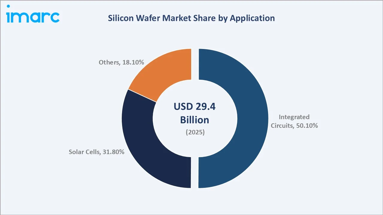
Solar Cells represent 31.8% of silicon wafer demand (2025), making solar the second-largest application category. According to the IEA PVPS, global cumulative solar PV capacity exceeded 2.2 terawatts (TW) by the end of 2024, rising from 1.6 TW in 2023, driven by the addition of more than 600 GW of new installations during the year.
Regional Market Insights
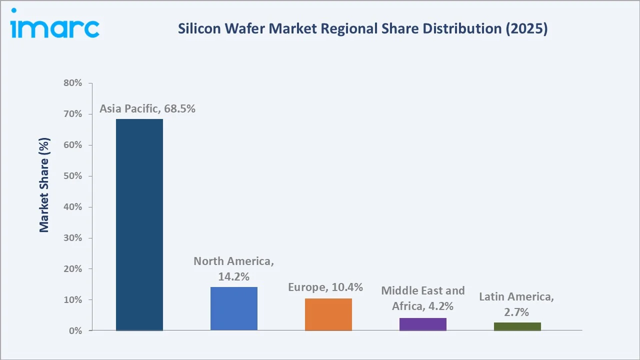
Asia Pacific's extraordinary 68.5% market share (2025) reflects a decades-long accumulation of semiconductor manufacturing infrastructure, workforce expertise, and supply chain density unique in global industrial history. South Korea's Samsung and SK Hynix are the world's largest DRAM and NAND flash producers, creating massive captive demand for SK Siltron's wafer output.
|
Region |
Share (2025) |
Key Growth Drivers |
Regulatory Impact |
Major Players |
|
Asia Pacific |
68.5% |
TSMC/Samsung fab density, China domestic fab investment, solar PV |
China MIIT guidelines; Korea K-Chips Act; Japan METI |
Shin-Etsu, SUMCO, SK Siltron, NSIG, GlobalWafers (Taiwan) |
|
North America |
14.2% |
CHIPS Act USD 52.7B, Intel/TSMC Arizona fabs, AI chip demand |
CHIPS Act incentives; export controls on advanced tech |
GlobalWafers Texas plant, Soitec (SOI), Pure Wafer |
|
Europe |
10.4% |
TSMC Dresden, Intel Germany; EU Chips Act EUR 43B commitment |
EU Chips Act; GDPR semiconductor IP protection |
Siltronic AG (Germany), Soitec (France), Okmetic (Finland) |
|
Middle East and Africa |
4.2% |
Saudi Vision 2030 semiconductor ambitions; UAE tech hub growth |
NEOM digital infrastructure policies |
Emerging; limited current wafer manufacturing |
|
Latin America |
2.7% |
Brazil semiconductor initiative; Mexico nearshoring electronics |
Brazil PNM semiconductor program |
Primarily import-dependent; emerging ecosystem |
North America (14.2% share, 2025) is undergoing a structural transformation driven by the CHIPS & Science Act's USD 52.7 Billion investment commitment and consequential announcements of TSMC Arizona (USD 65 Billion), and Samsung Texas (USD 25 Billion) manufacturing investments. ZMC's November 2024 acquisition of Pure Wafer is the anchor domestic wafer supply investment matching this historic fab buildout wave.
Competitive Landscape
Five incumbent manufacturers- Shin-Etsu Chemical, SUMCO, GlobalWafers, Siltronic, and SK Siltron- controlled approximately 85% of global 300mm silicon wafer capacity in 2025, reflecting the multi-billion dollar capital barriers, proprietary crystal-pulling expertise, and long-term customer qualification relationships that characterize this highly concentrated industry.
|
Company Name |
Headquarters |
Market Position |
Core Strength |
|
Shin-Etsu Chemical Co. Ltd. |
Tokyo, Japan |
Global Market Leader |
Largest 300mm capacity; vertically integrated; approx. 27% global share |
|
SUMCO Corporation |
Tokyo, Japan |
Global Market Leader |
Ultra-high-purity CZ crystal expertise; advanced MCZ AI-grade wafers; approx. 24% |
|
GlobalWafers Co. Ltd. |
Hsinchu, Taiwan |
Strong Challenger |
Post-acquisition scale; USD 5B Texas 300mm plant; Americas supply security |
|
Siltronic AG |
Munich, Germany |
European Leader |
Precision 300mm epi and polished wafers; European foundry supply partner |
|
SK Siltron Co. Ltd. |
Gumi, South Korea |
Asia Challenger |
SK Group semiconductor ecosystem integration; SiC wafer commercialization |
|
Wafer Works Corporation |
Taoyuan, Taiwan |
Regional Player |
Taiwan domestic supply; 200mm specialty wafer expertise |
|
Virginia Semiconductor Inc. |
Virginia, U.S. |
Niche / Specialty Wafer Manufacturer |
Specializing in small-diameter (1–150mm) wafers and specialty substrates, including limited SOI production |
The silicon wafer market exhibits characteristics of a natural oligopoly: technology barriers to entry are extraordinarily high, customer qualification cycles for new wafer suppliers span 2-4 years, and the precision manufacturing expertise required for sub-angstrom surface finish quality takes decades to develop organically.
Key Company Profiles
Shin-Etsu Chemical Co. Ltd.
Shin-Etsu Chemical is the world’s largest silicon wafer manufacturer, consistently holding a leading share of the global semiconductor silicon wafer market. The company operates advanced wafer manufacturing facilities in Japan and Singapore, producing a broad portfolio of high-performance wafers for leading semiconductor applications.
- Product Portfolio: 300mm and 200mm polished wafers, epitaxial wafers, silicon-on-insulator (SOI) wafers, and specialty wafers for power and advanced logic applications.
- Recent Developments: Shin-Etsu continues to expand its 300mm wafer capacity, particularly in Singapore and Japan, to support growing demand from advanced logic and memory nodes, including AI and high-performance computing applications.
- Strategic Focus: Leadership in ultra-flat, high-specification 300mm wafers, expansion of global manufacturing footprint, and development of advanced materials for next-generation semiconductor devices.
SUMCO Corporation
SUMCO is one of the world’s leading silicon wafer manufacturers and a key supplier to global semiconductor companies, with FY2024 revenues of approximately JPY 396.6 billion. The company is recognized for its advanced crystal growth technologies, including CZ, MCZ, and FZ processes, which enable high-quality wafers for memory and logic applications.
- Product Portfolio: 300mm polished and epitaxial wafers, MCZ wafers optimized for DRAM, SOI wafers, and specialty wafers for power devices and sensors.
- Recent Developments: SUMCO has announced the gradual phase-out of 200mm and smaller wafer production at its Miyazaki plant by the end of 2026, reflecting a strategic shift toward higher-margin 300mm wafer production.
- Strategic Focus: Expansion of 300mm wafer capacity, strengthening of advanced node wafer capabilities, and close co-development with leading memory and logic semiconductor manufacturers.
GlobalWafers Co., Ltd.
GlobalWafers, headquartered in Hsinchu, Taiwan, is the world’s third-largest silicon wafer manufacturer, with a strong global footprint across Asia, Europe, and North America. The company has expanded significantly through acquisitions and continues to invest in new capacity to support semiconductor supply chain resilience.
- Product Portfolio: 300mm and 200mm polished wafers, epitaxial wafers, and specialty wafers across multiple diameters for a wide range of semiconductor applications.
- Recent Developments: The company is developing a major 300mm wafer manufacturing facility in Sherman, Texas, representing one of the most significant silicon wafer investments in the United States in decades, supported by CHIPS Act funding.
- Strategic Focus: Strengthening regional supply chains, particularly in North America, expanding advanced wafer capacity, and supporting leading-edge semiconductor manufacturing for AI, automotive, and high-performance computing applications.
Market Concentration Analysis
The silicon wafer market is one of the most concentrated in the global materials industry. The top-5 producers - Shin-Etsu Chemical (approx. 27%), SUMCO (approx. 24%), GlobalWafers (approx. 17%), Siltronic (approx. 12%), and SK Siltron (approx. 9%) - collectively controlled approximately 89% of global 300mm wafer revenue in 2025.
Chinese challengers - National Silicon Industry Group (NSIG), Shanghai Simgui Technology, and Zhonghuan Advanced Semiconductor Materials - are targeting mature-grade wafers where the technology gap with Japanese and Korean leaders is smaller. These Chinese producers are pricing 10-15% below Japanese peers to win share in domestic automotive and industrial fabs.
Specialty niches represent the most fragmented sub-segments. Soitec's Smart Cut SOI technology commands over 70% of the global SOI wafer market, where its proprietary patent portfolio creates sustainable competitive moats. The FZ wafer segment for power electronics, radiation detectors, and high-resistivity applications is served by specialty producers including Topsil and Okmetic, commanding significant price premiums over standard CZ wafers.
Investment & Growth Opportunities
Fastest Growing Segments
AI and HPC wafer demand (CAGR approximately 11.3%), N-type wafer transition in solar (CAGR approximately 7.2%), and advanced packaging silicon interposer demand (CAGR approximately 35% from a small base) represent the highest-growth investment vectors through 2034.
Emerging Market Expansion
India's semiconductor manufacturing ambition - anchored by the Tata Electronics/Powerchip fab in Dholera, Gujarat (INR 91,000 Crore approved in March 2024) and the CG Power/Renesas assembly and test facility - is creating the foundation for future domestic silicon wafer demand. Saudi Arabia's NEOM digital city and Vision 2030 semiconductor initiatives represent emerging market investments that could create new silicon wafer consumption centers by the early 2030s.
Venture and Strategic Investment Trends
- Government subsidies are creating unprecedented incentives for silicon wafer capacity investment across the US, EU, Japan, South Korea, and India. Total government semiconductor support across these five geographies exceeds USD 250 billion through 2030, the largest technology industrial policy investment in history.
- SiC and GaN adjacency investments represent a USD 8-12 billion incremental market opportunity for silicon wafer producers with compound semiconductor capabilities, driven by EV power electronics and renewable energy power conversion demand through 2034.
- Advanced packaging silicon interposer demand is growing at a fast pace, creating a high-margin niche for premium ultra-thin silicon wafer producers with the precision thickness control and electrical uniformity specifications required for 2.5D and 3D-IC packaging architectures targeting AI chip customers.
Future Market Outlook (2026-2034)
The global silicon wafer market is positioned for its most robust sustained growth cycle in decades, driven by the AI hardware revolution and the structural nationalization of semiconductor supply chains through government investment programs. From a projected base of USD 29.4 Billion in 2025, the market is forecast to reach USD 47.0 Billion by 2034, representing absolute incremental value creation of USD 17.6 Billion, equivalent to adding an entirely new market the size of today's 300mm logic wafer segment over the forecast period.
Technological disruptions shaping the market through 2034 include the commercialization of gate-all-around (GAA) transistors at 2nm nodes, the potential emergence of silicon photonics as a data center interconnect standard driving ultra-low-defect optical silicon wafer demand, and the scaling of silicon-based quantum computing platforms requiring near-perfect crystalline silicon substrates with parts-per-trillion impurity control.
The geopolitical dimension of the silicon wafer market will intensify through 2034, with US-China technology decoupling accelerating the development of parallel, partially isolated semiconductor supply chains across Western-aligned and China-domestic ecosystems. This bifurcation will create geographic market segmentation, pricing divergence between supply-chain-aligned wafer contracts and spot market transactions, and strategic inventory behavior as fabs seek to build wafer buffer stocks against geopolitical supply disruptions.
Research Methodology
Primary Research
Primary research for this report included structured interviews with over 140 semiconductor industry professionals in 2024-2025, comprising silicon wafer manufacturing executives, semiconductor fab procurement directors, equipment engineers, materials scientists, and institutional investors across Japan, South Korea, Taiwan, the U.S., and Germany.
Secondary Research
Secondary research encompassed review of company annual reports from Shin-Etsu Chemical, SUMCO, GlobalWafers, Siltronic, SK Siltron, and Soitec; government semiconductor investment program documentation (CHIPS Act, EU Chips Act, METI strategy documents); SEMI equipment billing data; WSTS semiconductor shipment statistics; and industry trade publications (Semiconductor Engineering, EE Times, VLSI Research).
Forecasting Models
Market size estimates and CAGR projections were derived through a bottom-up wafer demand modeling approach, aggregating fab-level capacity expansion plans, technology node transition timelines, and wafer start per chip demand curves across 25+ semiconductor device application categories. A top-down validation using GDP growth rates, semiconductor market projections, and historical silicon wafer-to-semiconductor revenue intensity ratios was applied as a cross-check.
Silicon Wafer Market Report Scope:
| Report Features | Details |
|---|---|
| Base Year of the Analysis | 2025 |
| Historical Period | 2020-2025 |
| Forecast Period | 2026-2034 |
| Units | Billion USD |
| Scope of the Report |
Exploration of Historical Trends and Market Outlook, Industry Catalysts and Challenges, Segment-Wise Historical and Future Market Assessment:
|
| Wafer Sizes Covered | 300mm, 200mm, 150mm, Others |
| Types Covered | P-type, N-type |
| Applications Covered | Integrated Circuits, Solar Cells, Others |
| End Uses Covered | Solar, Consumer Electronics, Telecommunications, Automotive, Industrial, Others |
| Regions Covered | Asia Pacific, Europe, North America, Latin America, Middle East and Africa |
| Countries Covered | United States, Canada, Germany, France, United Kingdom, Italy, Spain, Russia, China, Japan, India, South Korea, Australia, Indonesia, Brazil, Mexico |
| Companies Covered | Shin-Etsu Chemical Co. Ltd., SUMCO Corporation, GlobalWafers Co. Ltd., Siltronic AG, SK Siltron Co. Ltd., Wafer Works Corporation, Virginia Semiconductor Inc., etc. |
| Customization Scope | 10% Free Customization |
| Post-Sale Analyst Support | 10-12 Weeks |
| Delivery Format | PDF and Excel through Email (We can also provide the editable version of the report in PPT/Word format on special request) |
Key Benefits for Stakeholders:
- IMARC’s report offers a comprehensive quantitative analysis of various market segments, historical and current market trends, market forecasts, and dynamics of the silicon wafer market from 2020-2034.
- The silicon wafer market research report provides the latest information on the market drivers, challenges, and opportunities in the global market.
- The study maps the leading, as well as the fastest-growing, regional markets. It further enables stakeholders to identify the key country-level markets within each region.
- Porter's five forces analysis assist stakeholders in assessing the impact of new entrants, competitive rivalry, supplier power, buyer power, and the threat of substitution. It helps stakeholders to analyze the level of competition within the silicon wafer industry and its attractiveness.
- Competitive landscape allows stakeholders to understand their competitive environment and provides an insight into the current positions of key players in the market.
Frequently Asked Questions About the Silicon Wafer Market Report
The global market was valued at USD 29.4 Billion in 2025 and is projected to reach USD 47.0 Billion by 2034, growing at a CAGR of 5.36%.
The silicon wafer market is expected to grow at a CAGR of 5.36% during 2026-2034, driven by AI chip demand, 5G infrastructure build, EV semiconductor expansion, and government fab investment programs globally.
P-type silicon wafers lead with a 57.1% market share in 2025, reflecting their entrenched position in CMOS logic, DRAM, NAND flash, and analog semiconductor manufacturing processes globally.
Integrated circuits lead with a 50.1% application share in 2025, driven by logic processors, memory chips, AI accelerators, and power semiconductors for consumer electronics, data centers, and automotive applications.
Asia Pacific dominates with a 68.5% market share in 2025, anchored by Japan's Shin-Etsu and SUMCO wafer manufacturers, Taiwan's TSMC fab demand, and South Korea's Samsung and SK Hynix semiconductor output.
Key drivers include AI and HPC chip demand, electric vehicle semiconductor content growth, 5G infrastructure expansion, the government CHIPS Act and EU Chips Act fab investments, and IoT device proliferation across multiple industries.
The top-5 players, Shin-Etsu Chemical, SUMCO, GlobalWafers, Siltronic AG, and SK Siltron, collectively control approximately 85% of global 300mm wafer capacity. Soitec leads the specialty SOI wafer segment globally.
AI and HPC-grade wafers are growing at approximately 11.3% CAGR, while N-type wafers are expanding at 7.2% CAGR, driven by solar PV efficiency transitions (TOPCon, HJT) and advanced logic node adoption through 2034.
The USD 52.7 billion CHIPS Act is funding 40+ new US semiconductor fabs, creating significant incremental domestic wafer demand. GlobalWafers received USD 406 million in CHIPS grants for its USD 5 billion Texas 300mm wafer plant.
Key challenges include high capital intensity for new capacity, geopolitical supply chain concentration in East Asia, polysilicon price volatility, and stringent defect density requirements at sub-2nm process technology nodes.
High-growth opportunities include AI-grade 300mm wafer capacity expansion, N-type wafer transition in solar PV, silicon interposer demand for advanced packaging, and government-backed domestic wafer manufacturing in the U.S., Europe, and India.
Need more help?
- Speak to our experienced analysts for insights on the current market scenarios.
- Include additional segments and countries to customize the report as per your requirement.
- Gain an unparalleled competitive advantage in your domain by understanding how to utilize the report and positively impacting your operations and revenue.
- For further assistance, please connect with our analysts.
 Request Customization
 Speak to an Analyst
 Request Brochure
 Inquire Before Buying
Benefits of Customization
- Personalize this research
- Triangulate with your data
- Get data as per your format and definition
- Gain a deeper dive into a specific application, geography, customer, or competitor
- Any level of personalization
Get in Touch With Us
UNITED STATES
Phone: +1-201-971-6302
INDIA
Phone: +91-120-433-0800
UNITED KINGDOM
Phone: +44-753-714-6104
Email: [email protected]
Client Testimonials

.webp)