
Japan Semiconductor Manufacturing Equipment Market Size, Share, Trends and Forecast by Equipment Type, Product Type, Dimension, Supply Chain Participant, and Region, 2026-2034
Japan Semiconductor Manufacturing Equipment Market Size, Share, Trends & Forecast (2026-2034)
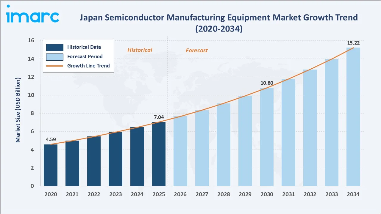
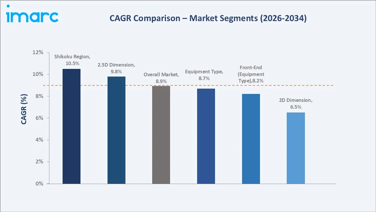
The Japan semiconductor manufacturing equipment market reached USD 7.04 Billion in 2025 and is projected to reach USD 15.22 Billion by 2034, exhibiting a robust CAGR of 8.93% during 2026-2034. Japan is one of the world's foremost semiconductor equipment hubs, home to globally dominant OEMs such as Tokyo Electron Ltd. (TEL) and Advantest Corporation. The market is propelled by accelerating adoption of extreme ultraviolet (EUV) lithography, proliferating demand for electric and hybrid vehicles (H/EVs), and the nationwide push for domestic semiconductor self-sufficiency under METI-backed programs.
Market Snapshot
|
Metric |
Value |
|
Market Size (2025) |
USD 7.04 Billion |
|
Forecast Market Size (2034) |
USD 15.22 Billion |
|
CAGR (2026-2034) |
8.93% |
|
Base Year |
2025 |
|
Historical Period |
2020-2025 |
|
Forecast Period |
2026-2034 |
|
Largest Region (2025) |
Kanto Region (35.8%) |
|
Fastest Growing Region |
Kyushu-Okinawa Region |
|
Largest Dimension |
2D (46.2%) |
|
Largest Equipment Type |
Front-End (62.8%) |
Figure 1 below illustrates the market growth trajectory from 2020 to 2034, with 2025 as the base year. The trend is set to sustain through the forecast horizon.
To get more information on this market, Request Sample
The CAGR growth curve (Figure 2) confirms a sharp inflection from 2026, as next-generation node transitions and the greenfield Rapidus sub-2nm fab project in Hokkaido are expected to catalyze incremental equipment orders exceeding USD 4 Billion cumulatively through 2034.
Executive Summary
Japan's semiconductor manufacturing equipment market reached USD 7.04 Billion in 2025, building upon a 2020 base of USD 4.59 Billion at a historical CAGR of approximately 8.9%. Looking ahead, the market is forecast to more than double to USD 15.22 Billion by 2034, driven by the convergence of multiple structural forces. These include the rapid miniaturization of semiconductor nodes, the explosion of connected devices embedded in consumer electronics and automotive platforms, and Japan's decisive policy pivot towards domestic chip manufacturing self-reliance.
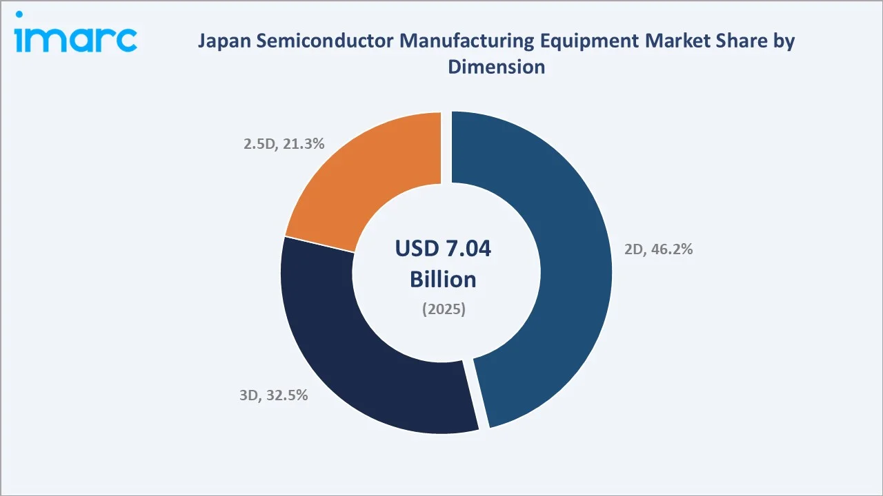
The front-end equipment segment retained its commanding position at 62.8% of market share in 2025, underpinned by continuous capital expenditure at memory, logic, and advanced node fabs located primarily in the Kanto and Kansai corridors. The 2D dimension segment led at 46.2% in 2025, reflecting the volume-driven legacy node production serving consumer electronics and automotive sectors. However, the 3D segment at 32.5% is gaining traction rapidly, as chipmakers integrate high-bandwidth memory (HBM) and 3D-IC architectures for AI accelerators and data center applications.
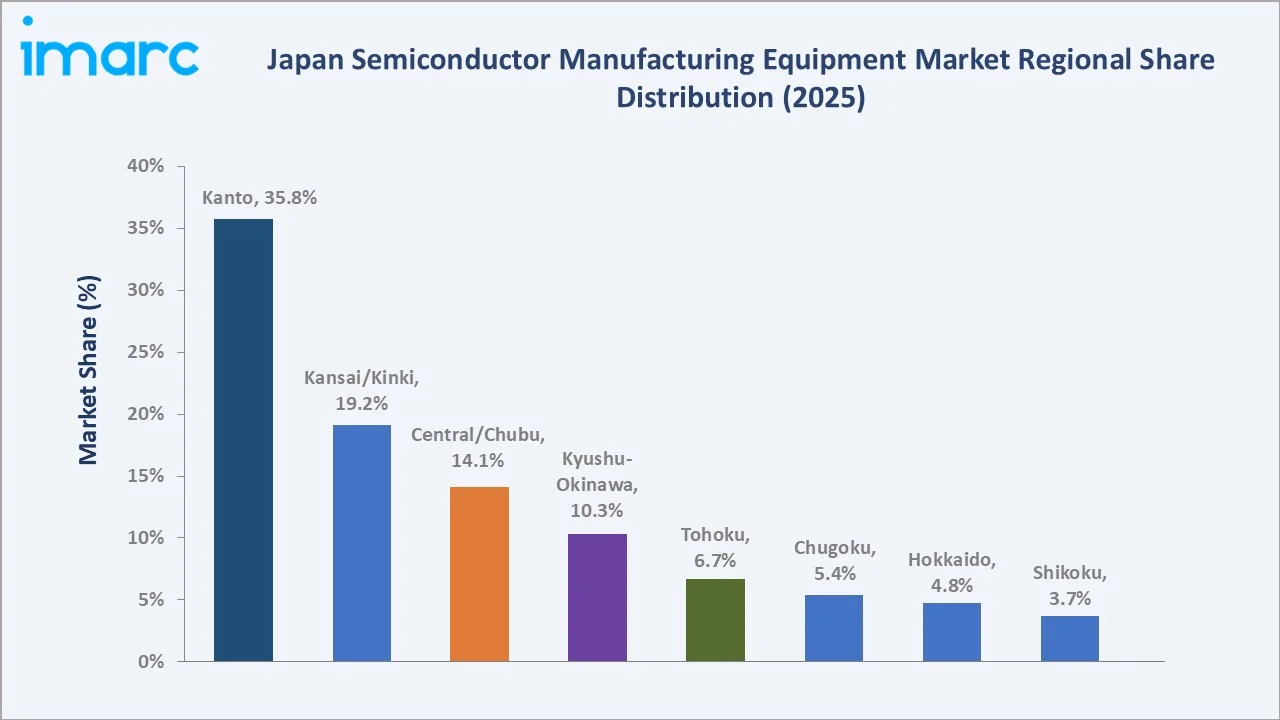
The Kanto Region, anchored by Tokyo and its surrounding industrial cluster, dominated with a 35.8% share in 2025. Meanwhile, the Kyushu-Okinawa Region is emerging as the fastest-growing zone, catalyzed by TSMC's Kumamoto fab ramp-up and substantial METI investment.
Key Market Insights
|
Insight |
Data |
|
Largest Dimension |
2D – 46.2% share in 2025 |
|
Largest Equipment Type |
Front-End Equipment – 62.8% in 2025 |
|
Leading Region |
Kanto Region – 35.8% share in 2025 |
|
Fastest Growing Region |
Kyushu-Okinawa Region |
|
Top Companies |
Tokyo Electron Limited., Advantest Corporation, KOKUSAI ELECTRIC CORPORATION, Hitachi, Ltd., ULVAC, DISCO CORPORATION |
|
Market Opportunity |
Sub-2nm node equipment and advanced packaging upgrades |
The Following Bullet Insights Expand on the Key Data Points Outlined Above:
- 2D dimension equipment led the Japan semiconductor equipment market in 2025 with a 46.2% share, driven by high-volume legacy-node production for consumer electronics, automotive MCUs, and analog ICs that continue to demand planar process equipment.
- Front-end equipment dominated with 62.8% share in 2025 as lithography, deposition, etch, and wafer conditioning tools constitute the capital-intensive core of every advanced fab build-out in Japan's Kanto and Kansai regions.
- The Kanto Region contributed 35.8% of market revenue in 2025 – the single largest regional share – owing to the concentration of TEL's R&D campus, Hitachi, Ltd. headquarters, and multiple Samsung, SK Hynix, and Micron-affiliated equipment test sites.
- The Kyushu-Okinawa Region, holding a 10.3% share in 2025, is identified as the fastest-growing region through 2034, propelled by TSMC's Phase 1 (6nm) and Phase 2 (3nm) fabs at Kumamoto, representing a combined equipment spend of over USD 25 Billion.
- Rapidus Corporation's sub-2nm project in Hokkaido (4.8% regional share in 2025) is positioned to become a transformative demand anchor for EUV scanners, atomic layer deposition (ALD) tools, and advanced metrology equipment from 2026 onwards.
- The 3D dimension segment held 32.5% market share in 2025 and is expected to record the highest CAGR through 2034, as AI-driven HBM and 3D-NAND packaging technologies require specialized bonding, through-silicon-via (TSV), and stacking equipment.
Japan Semiconductor Manufacturing Equipment Market Overview
Semiconductor manufacturing equipment encompasses the machinery deployed to fabricate integrated circuits (ICs) and electronic components from raw silicon wafers to finished semiconductor devices. This equipment spectrum spans front-end processes – including photolithography, chemical vapor deposition (CVD), physical vapor deposition (PVD), dry and wet etching, ion implantation, and chemical mechanical planarization (CMP) – through to back-end processes such as wafer dicing, die bonding, wire bonding, encapsulation, and functional testing. Fab facility equipment, constituting 12.6% of the Japan market in 2025, supports the clean-room environment through advanced gas and chemical control, automation, and environmental management systems.
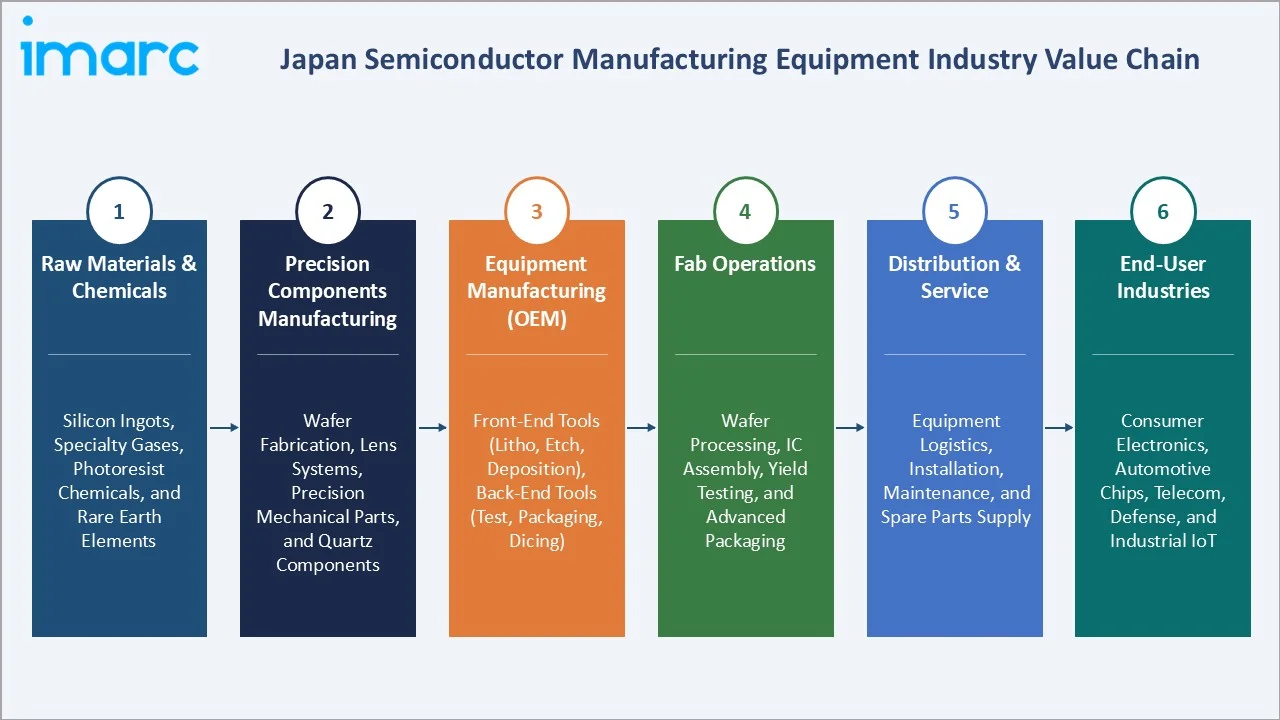
Japan's semiconductor equipment ecosystem is deeply integrated with global semiconductor supply chains, with domestic OEMs supplying critical tools to fabs across East Asia, North America, and Europe. Macroeconomic factors, and alignment with the US CHIPS and Science Act – have accelerated fab investment decisions. Furthermore, the post-pandemic surge in silicon demand across automotive, consumer electronics, and data center verticals has driven capacity expansion projects at multiple Japanese fabs.
Market Dynamics
To evaluate market opportunities, Request Sample
Market Drivers
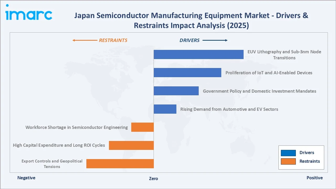
- Rising Demand from Automotive and EV Sectors: Japan’s automotive semiconductor demand has grown strongly in recent years, as hybrid and electric vehicle (H/EV) production by Toyota, Honda, and Nissan increasingly relies on power electronics, LIDAR chips, and advanced driver-assistance system (ADAS) components that require state-of-the-art fabrication equipment.
- Government Policy and Domestic Investment Mandates: Japan’s Semiconductor and Digital Industry Strategy (2023) allocate substantial funding toward domestic semiconductor manufacturing, directly stimulating demand for front-end and back-end equipment from both domestic OEMs and global suppliers seeking to establish Japan-based service centers.
- Proliferation of IoT and AI-Enabled Devices: Growth in industrial automation, smart infrastructure, and connected devices increases the need for high-performance chips, boosting investment in semiconductor fabrication and advanced equipment such as lithography, deposition, and inspection systems across domestic manufacturing facilities.
- EUV Lithography and Sub-3nm Node Transitions: The shift from DUV to EUV lithography – enabling feature sizes below 7nm – is driving a capital equipment upgrade cycle across Japanese fabs. Each EUV scanner (used in advanced semiconductor manufacturing equipment ecosystem development) triggers ancillary spending on compatible resist systems, metrology tools, and environmental controls.
Market Restraints
- Export Controls and Geopolitical Tensions: Japan aligned with US and Dutch export restrictions on advanced semiconductor manufacturing tools to China, curtailing a historically significant revenue stream. Japan’s exports of semiconductor manufacturing equipment to China declined in the subsequent period due to tightened controls on advanced technology shipments.
- High Capital Expenditure and Long ROI Cycles: Advanced semiconductor fabs require very high capital investments per facility, creating significant financial barriers for new entrants and extending equipment procurement cycles to multiple years, thereby dampening near-term order velocity.
- Workforce Shortage in Semiconductor Engineering: Japan’s semiconductor equipment market faces a constraint due to a shortage of skilled semiconductor engineers. Limited talent availability slows fab expansion, delays equipment installation and optimization, and reduces overall utilization efficiency.
Market Opportunities
- Rapidus Sub-2nm Program: Rapidus Corporation’s IBM-partnered fab in Chitose, Hokkaido, targeting 2nm chip production by 2027, represents a generational equipment demand opportunity. The project is expected to require very large-scale investment, with a significant share directed toward Japanese and international semiconductor equipment suppliers.
- Advanced Packaging Equipment Demand: The global transition to 2.5D and 3D-IC packaging architectures for AI accelerators and HBM modules is creating a significant annual equipment opportunity in Japan by 2030, particularly for bonding systems, TSV drilling tools, and wafer-level packaging inspection equipment.
- Expansion of Memory Fab Capacity: Kioxia (formerly Toshiba Memory) and its alliance with Western Digital continue to invest in NAND Flash capacity expansion at Yokkaichi and Kitakami fabs, driving multi-billion-dollar equipment procurement cycles through 2028.
Market Challenges
- Supply Chain Disruptions for Critical Materials: Specialty gases (e.g., neon, krypton, xenon) and rare earth materials critical to photolithography and deposition processes remain geographically concentrated, exposing Japanese equipment manufacturers to supply chain vulnerabilities and cost volatility.
- Technology Leapfrogging Risk: The rapid pace of semiconductor innovation – moving toward gate-all-around (GAA) transistor architectures and beyond-Si materials such as GaN and SiC – demands continuous R&D reinvestment from equipment manufacturers. Falling behind on a single node transition can trigger a multi-year revenue gap.
- Competition from Korean and US Equipment Suppliers: While Japan is home to TEL (the world's second-largest semiconductor equipment company by revenue), global competitors such as ASML (Netherlands), Applied Materials (US), and Lam Research (US) maintain strong market positions in Japan's leading fabs through long-term supply agreements.
Emerging Market Trends
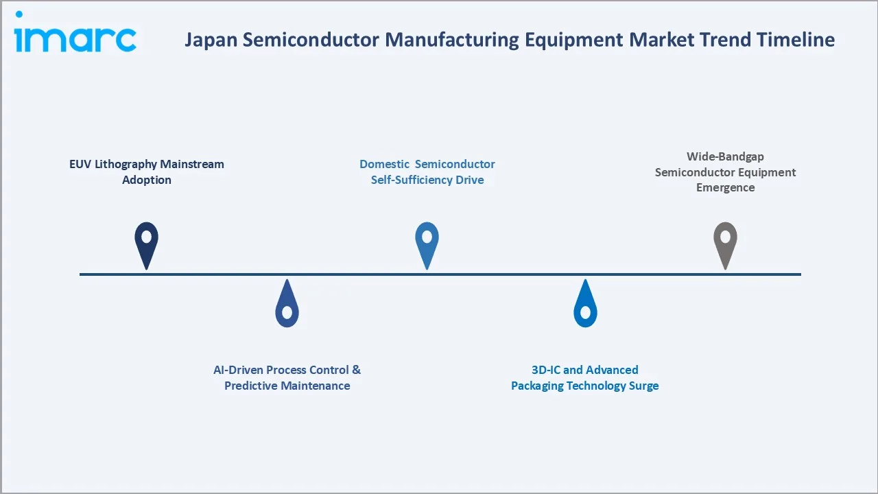
1: EUV Lithography Mainstream Adoption
EUV lithography systems are increasingly deployed at Japan’s leading fabs, including advanced memory and logic manufacturing lines. The installed base is growing steadily, with next-generation high-NA EUV systems expected to enter Japanese fabs in the late 2020s, enabling sub-2nm patterning and driving broader equipment upgrades across deposition, etch, and inspection categories.
2: AI-Driven Process Control and Predictive Maintenance
Equipment manufacturers including TEL and Hitachi High-Tech are embedding AI and machine learning capabilities into process control modules. AI-enabled defect detection systems have demonstrated measurable yield improvements in pilot deployments at Japanese fabs in recent years. Predictive maintenance platforms using IoT-enabled sensors on critical process tools are also reducing unplanned downtime, while creating new service-based revenue streams for OEMs.
3: 3D-IC and Advanced Packaging Technology Surge
The 3D-IC and advanced packaging segment—including CoWoS, EMIB, and hybrid bonding technologies—has been growing rapidly in Japan in recent years. Key players such as Sony’s image sensor division, TSMC’s Kumamoto operations, and emerging OSAT providers are investing in advanced packaging capacity, directly increasing demand for die-attach equipment, flip-chip bonding systems, and wafer-level packaging tools from leading suppliers such as Disco Corporation and ULVAC.
4: Domestic Semiconductor Self-Sufficiency Drive
Japan’s semiconductor strategy aims to strengthen domestic chip manufacturing and expand its share of global semiconductor production value by 2030 compared to earlier levels. This policy push is driving committed capital expenditure from domestic fabs and attracting foreign direct investment from global chipmakers, collectively creating a sustained multi-year equipment procurement cycle expected to reach tens of billions of dollars through 2030.
Trend 5: Wide-Bandgap Semiconductor Equipment Emergence
Growing automotive and power electronics applications are fueling demand for SiC and GaN wafer processing equipment in Japan. ROHM Semiconductor and Mitsubishi Electric are expanding SiC epitaxy and fabrication lines, creating incremental demand for specialized CVD reactors and implant tools not typically required for silicon processing.
Industry Value Chain Analysis
|
Stage |
Key Activities |
|
Raw Materials & Chemicals |
Silicon ingots, specialty gases, photoresist chemicals, rare earth elements |
|
Precision Components Mfg. |
Wafer fabrication, lens systems, precision mechanical parts, quartz components |
|
Equipment Manufacturing (OEM) |
Front-end tools (litho, etch, deposition), back-end (test, packaging, dicing) |
|
Fab Operations & Integration |
Wafer processing, IC assembly, yield testing, advanced packaging |
|
Distribution & After-Sales |
Equipment logistics, installation, maintenance, spare parts supply |
|
End-User Industries |
Consumer electronics, automotive chips, telecom, defense, industrial IoT |
The Japan semiconductor manufacturing equipment value chain spans six integrated stages, from upstream raw material extraction through to downstream end-user deployment. Each stage represents both a cost center and an innovation opportunity, with Japanese companies occupying dominant positions across multiple layers – providing a structural competitive advantage.
Technology Landscape in the Japan Semiconductor Manufacturing Equipment Industry
Advanced Lithography Systems
EUV and deep UV immersion lithography remain cornerstone technologies in Japan’s front-end semiconductor equipment landscape. TEL’s CLEAN TRACK lithography coater-developers hold a dominant share of the domestic photoresist application systems market. Japan’s METI has also supported development of next-generation photomask technologies and EUV resist materials through partnerships between leading materials companies such as Shin-Etsu Chemical and JSR Corporation.
Atomic-Level Deposition and Etch Technologies
Atomic layer deposition (ALD) and atomic layer etch (ALE) technologies are gaining primacy as device nodes shrink below 5nm. ULVAC's ALD systems demonstrated a film thickness uniformity of ±0.5% in high-volume production settings in 2024. Kokusai Electric's thermal processing and ALD batch systems serve leading DRAM manufacturers including Micron's Hiroshima fab, processing 300mm wafers at throughputs exceeding 100 wafers per hour.
AI-Integrated Metrology and Inspection Tools
Hitachi High-Tech’s SEM (scanning electron microscope) systems incorporate AI-based defect classification, reducing inspection cycle times compared to traditional rule-based approaches. The global semiconductor metrology and inspection equipment market is substantial, with Japan-based vendors holding a significant share. In-line critical dimension (CD) metrology tools now enable extremely high-precision measurement at the atomic scale, supporting advanced node semiconductor manufacturing.
Smart Automation and Digital Twin Integration
Factory automation within Japanese semiconductor fabs has reached very high levels of material handling automation at leading facilities. Digital twin platforms are being deployed by major equipment and technology providers to simulate process flows and equipment behavior before physical execution, helping reduce development time for new semiconductor nodes. The integration of private 5G networks within fab environments is further enabling real-time data analytics, predictive control, and remote equipment diagnostics.
Market Segmentation Analysis
The report covers the following segments:
| Segment Category | Leading Segment | Market Share | Year |
|---|---|---|---|
| Equipment Type | Front-End | 62.8% | 2025 |
| Product Type | 🔒 | 🔒 | 2025 |
| Dimension | 2D | 46.2% | 2025 |
| Supply Chain Participant | 🔒 | 🔒 | 2025 |
| Region | Kanto Region | 35.8% | 2025 |

Market Breakup by Dimension
To access detailed market analysis, Request Sample
The 2D segment dominated in 2025 with a 46.2% share, reflecting the continued high-volume production of conventional planar devices. 2D manufacturing remains the workhorse of commodity semiconductor categories including CMOS image sensors, discrete power devices, and standard logic chips that collectively sustain Japan's consumer electronics and industrial automation supply chains. The segment's relative maturity does not imply stagnation.
Market Breakup by Equipment Type
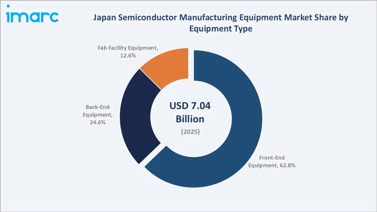
Front-end equipment commanded a 62.8% share in 2025, reflecting the capital intensity of wafer processing. Lithography tools, etch systems, and deposition equipment are the three largest sub-categories. Japan's TEL holds global top-3 positions in etch and deposition categories, while its coater-developer systems are deployed in virtually every major lithography line in the country.
Regional Market Insights
|
Region |
Share (2025) |
Key Drivers |
Regulatory Impact |
|
Kanto Region |
35.8% |
Tokyo fab cluster, major OEM HQs |
METI subsidies & CHIPS Act alignment |
|
Kansai/Kinki Region |
19.2% |
Osaka semiconductor corridor, legacy fabs |
Regional R&D incentives |
|
Central/Chubu Region |
14.1% |
Automotive chip demand, Nagoya cluster |
Auto sector regulations |
|
Kyushu-Okinawa Region |
10.3% |
TSMC fab presence, government-backed expansion |
JEITA & METI funding boost |
|
Tohoku Region |
6.7% |
Memory chip fabs, post-disaster rebuilding |
Local enterprise zones |
|
Chugoku Region |
5.4% |
Specialty chemicals, equipment testing |
Industrial safety norms |
|
Hokkaido Region |
4.8% |
Emerging tech parks, Rapidus sub-2nm fab |
Rapidus govt grant program |
|
Shikoku Region |
3.7% |
SME equipment suppliers, niche tools |
Regional manufacturing policy |
Japan's semiconductor manufacturing equipment market exhibits pronounced geographic concentration, with the Kanto Region alone contributing 35.8% of 2025 revenues. This concentration reflects decades of industrial clustering around Tokyo's technology corridor. However, policy-driven diversification is gradually redistributing fab and equipment investment toward southern and northern Japan.
Competitive Landscape
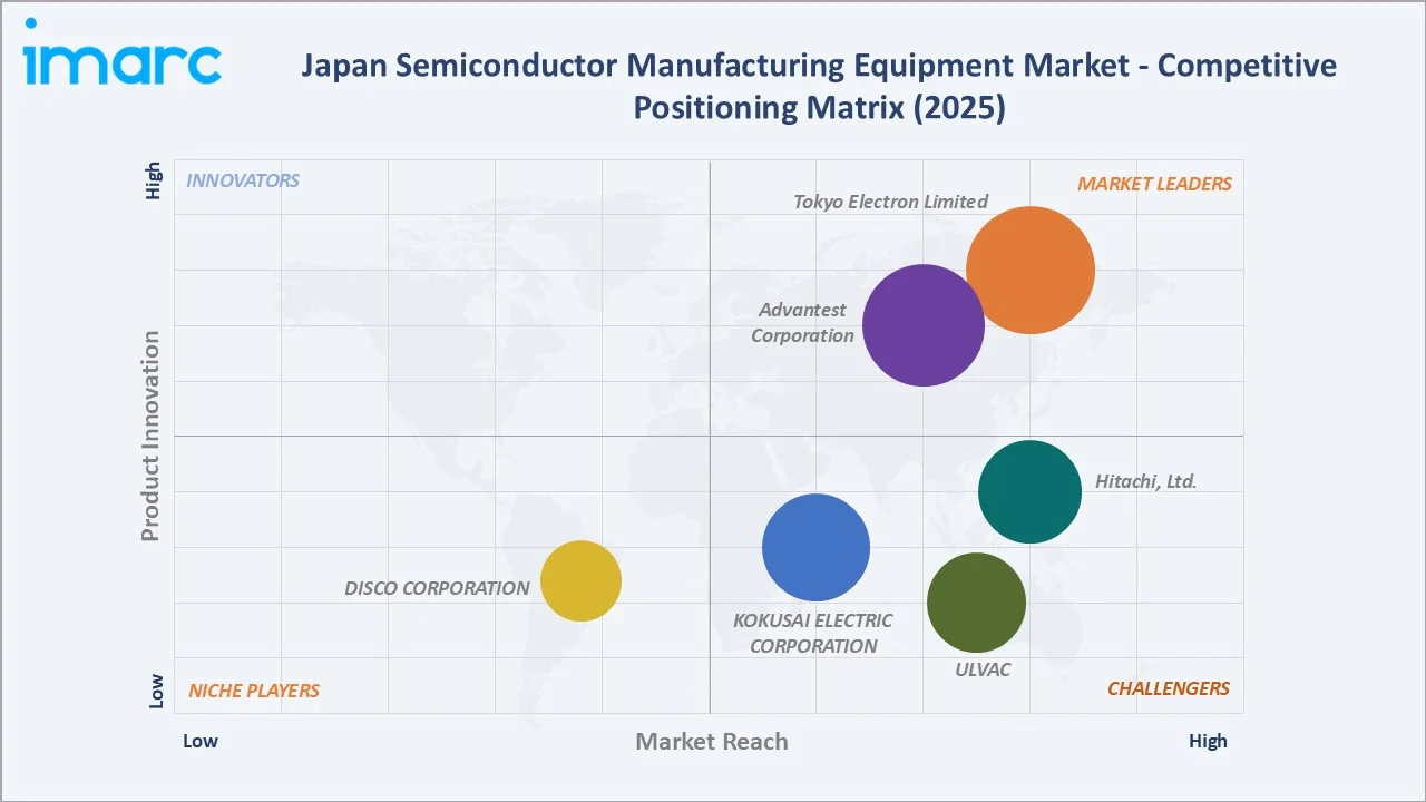
The Japan semiconductor manufacturing equipment market is moderately concentrated, with the top five players. The competitive landscape is shaped by deep technology moats, long-cycle customer relationships with major fabs, and high switching costs associated with process-qualified equipment portfolios.
|
Company Name |
Brand / Key Product Line |
Market Position |
Specialization |
|
Tokyo Electron Limited. |
CLEAN TRACK |
Leader |
Lithography, Etch, CVD Systems |
|
Advantest Corporation |
V93000 |
Leader |
Semiconductor Testing Systems |
|
KOKUSAI ELECTRIC CORPORATION |
VERTRON, QUIXACE |
Challenger |
Thermal Processing, ALD Equipment |
|
Hitachi, Ltd. |
SU Series |
Challenger |
SEM, Ion Beam, Metrology Tools |
|
ULVAC |
ENTRON |
Challenger |
Deposition & Vacuum Equipment |
|
DISCO CORPORATION |
DFD Series |
Emerging |
Dicing, Grinding, Polishing |
Global competitors maintain a significant presence in Japan through direct sales offices and long-term supply agreements.
Key Company Profiles
Tokyo Electron Ltd.
Tokyo Electron Ltd. is a Japan-based global leader in semiconductor manufacturing equipment, headquartered in Tokyo and founded in 1963. It is one of the world’s top suppliers of advanced chip fabrication tools, playing a critical role in the global semiconductor value chain.
- Product Portfolio: CLEAN TRACK coater-developers, Tactras etch systems, Triase+ oxidation/diffusion furnaces, Certas ALD/CVD systems, Vigus wafer cleaning systems, and ELTRAN SOI wafer bonding tools.
- Recent Developments: In 2021, Tokyo Electron Limited (TEL) announced a collaboration initiative aimed at advancing next-generation semiconductor manufacturing technologies, including EUV-related process development and ecosystem strengthening with global partners.
- Strategic Focus: TEL targets a doubling of revenue to through expansion in advanced logic, 3D-NAND, and DRAM equipment segments, with particular emphasis on gate-all-around (GAA) process tool development.
Advantest Corporation
Advantest Corporation is a Japan-based global leader in semiconductor test equipment, headquartered in Tokyo and founded in 1954. The company is one of the world’s largest suppliers of automatic test equipment (ATE) used to verify the performance, quality, and reliability of semiconductor devices.
- Product Portfolio: V93000 SoC test system, T5503 memory test system, W4900 wafer-level burn-in system, T2000 mixed-signal test platform, and MPT3000 parallel test solutions for HBM and DRAM.
- Recent Developments: In 2026, Advantest announced a strategic partnership with Applied Materials, strengthening cross-industry collaboration in semiconductor equipment innovation. The partnership focuses on integrating front-end manufacturing technologies with back-end semiconductor testing, aiming to accelerate development and commercialization of advanced chips and packaging solutions.
- Strategic Focus: Advantest is expanding its AI chip test portfolio to address the burgeoning demand from NVIDIA, AMD, and Amazon custom silicon programs, projecting test systems revenue from AI-related chips to surpass 30% of total revenue by FY2027.
Kokusai Electric Corporation
Kokusai Electric Corporation is a Japan-based semiconductor manufacturing equipment company specializing in advanced process technologies for chip fabrication. Headquartered in Tokyo, the company has a long legacy in the semiconductor industry and operates as a key supplier to leading global chipmakers.
- Product Portfolio: VERTRON series of 200-mm batch thermal processing systems, QUIXACEI-LV is a latest platform for batch thermal processing of 300mm wafers
- Recent Developments: In 2026, Kokusai Electric announced plans to acquire adjacent land near its Tonami Manufacturing Center in Toyama to support future expansion of semiconductor manufacturing equipment production and R&D capabilities.
- Strategic Focus: The company is accelerating development of single-wafer ALD systems for logic applications, targeting the growing foundry customer base at nodes below 3nm where batch-process tools are increasingly complemented by single-wafer precision.
Market Concentration Analysis
The Japan semiconductor manufacturing equipment market exhibits a moderately concentrated structure. The top five companies – Tokyo Electron Limited., Advantest Corporation, KOKUSAI ELECTRIC CORPORATION, Hitachi, Ltd., ULVAC – collectively accounted for an estimated 55%–60% of domestic market revenues in 2025.
The market fragmentation index (Herfindahl-Hirschman Index, HHI) is estimated in the moderately concentrated range, reflecting a competitive but not monopolistic environment. Niche equipment categories such as wafer dicing and certain ATE segments exhibit oligopolistic concentration. The fab facility equipment sub-segment is more fragmented, with numerous Japanese SME suppliers competing on specialized automation and gas control solutions.
Investment & Growth Opportunities
Fastest Growing Segments
The 3D dimension equipment segment is projected to record the highest CAGR within the Japan market through 2034, driven by HBM and 3D-NAND capacity additions. Back-end equipment – particularly advanced packaging and testing – is also forecast to outpace front-end growth rates post-2026 as chiplet and heterogeneous integration architectures proliferate.
Emerging Market Opportunities
The Kyushu-Okinawa Region presents the most compelling geographic investment opportunity, with TSMC's two Kumamoto fabs, Sony's sensor lines, and a growing OSAT cluster creating a multi-billion-dollar annual equipment procurement zone. The Hokkaido Rapidus project, targeting sub-2nm volume production by 2027–2028, represents a once-in-a-generation greenfield equipment demand event.
Venture Investment and M&A Trends
Japan’s Innovation Network Corporation and the Development Bank of Japan have collectively committed significant funding toward semiconductor technology investments in recent years. Private equity activity is also increasing, with global investors acquiring stakes in key semiconductor players, reflecting strong international confidence in Japan’s industry revival. Strategic M&A by major equipment manufacturers is expected to intensify, particularly in AI-driven process control, advanced packaging, and SiC-related technologies through the late 2027.
Future Market Outlook (2026-2034)
The Japan semiconductor manufacturing equipment market is poised for sustained, above-average growth through 2034. From USD 7.04 Billion in 2025, the market is forecast to reach USD 10.80 Billion by 2030 and USD 15.22 Billion by 2034, representing a cumulative increment of over USD 8 Billion across the forecast period. This trajectory is underpinned by three structural demand pillars: advanced node transitions requiring full tool refresh cycles, greenfield fab construction at TSMC Kumamoto Phase 2 and Rapidus Hokkaido, and the secular expansion of advanced packaging addressable equipment spend.
Technological disruption will be a key variable. The transition from EUV to high-NA EUV, the shift from FinFET to gate-all-around (GAA) transistor architectures at 3nm and below, and the emergence of backside power delivery networks (BSPDN) will collectively drive a new equipment super-cycle. TEL, Kokusai Electric, and Hitachi High-Tech are all aligned with these node transitions through multi-year joint development programs with TSMC and Rapidus.
Industry transformation will also manifest in the growing service revenue component: equipment-as-a-service (EaaS) models, and AI-driven process optimization subscriptions. This shift will improve revenue predictability and deepen customer stickiness for Japan's leading equipment manufacturers.
Research Methodology
Primary Research
Primary research for this report comprised structured interviews with senior executives and technical directors at leading semiconductor equipment OEMs, fab operators, and industry associations including JEITA (Japan Electronics and Information Technology Industries Association) and SEAJ (Semiconductor Equipment Association of Japan). A total of 45+ primary interviews were conducted across the research cycle, supplemented by expert panel consultations and proprietary surveys administered to fab procurement teams.
Secondary Research
Secondary research drew upon a comprehensive database of sources including: annual reports and investor presentations from TEL, Shin-Etsu Chemical, Advantest, and Kokusai Electric; regulatory filings with Japan's Ministry of Economy, Trade and Industry (METI) and the Financial Services Agency (FSA); industry publications from Gartner, IDC, VLSI Research, and IHS Markit; patent filings at the Japan Patent Office (JPO); and trade data from Japan's Ministry of Finance.
Forecasting Models
Market size estimates and forecasts were derived using a dual-approach methodology: (1) a bottom-up model aggregating equipment spend by fab project, node transition, and maintenance replacement cycles across all identified active and planned fabs in Japan; and (2) a top-down model applying Japan's estimated share of global semiconductor equipment spend (approximately 11%–13%) against IMARC Group's global semiconductor manufacturing equipment market baseline. Both approaches were cross-validated and reconciled to produce the published 2025–2034 forecast figures. CAGR calculations reflect compound annual growth from the 2025 base to the 2034 forecast year.
Japan Semiconductor Manufacturing Equipment Market Report Coverage:
| Report Features | Details |
|---|---|
| Base Year of the Analysis | 2025 |
| Historical Period | 2020-2025 |
| Forecast Period | 2026-2034 |
| Units | Billion USD |
| Scope of the Report | Exploration of Historical and Forecast Trends, Industry Catalysts and Challenges, Segment-Wise Historical and Predictive Market Assessment:
|
| Equipment Types Covered |
|
| Product Types Covered | Memory, Logic Components, Microprocessor, Analog Components, Optoelectronic Components, Discrete Components, Others |
| Dimensions Covered | 2D, 2.5D, 3D |
| Supply Chain Participants Covered | IDM Firms, OSAT Companies, Foundries |
| Regions Covered | Kanto Region, Kansai/Kinki Region, Central/ Chubu Region, Kyushu-Okinawa Region, Tohoku Region, Chugoku Region, Hokkaido Region, Shikoku Region |
| Companies Covered | Tokyo Electron Limited., Advantest Corporation, KOKUSAI ELECTRIC CORPORATION, Hitachi, Ltd., ULVAC, DISCO CORPORATION, etc. |
| Customization Scope | 10% Free Customization |
| Post-Sale Analyst Support | 10-12 Weeks |
| Delivery Format | PDF and Excel through Email (We can also provide the editable version of the report in PPT/Word format on special request) |
Key Benefits for Stakeholders:
- IMARC’s industry report offers a comprehensive quantitative analysis of various market segments, historical and current market trends, market forecasts, and dynamics of the Japan semiconductor manufacturing equipment market from 2020-2034.
- The research report provides the latest information on the market drivers, challenges, and opportunities in the Japan semiconductor manufacturing equipment market.
- Porter's five forces analysis assist stakeholders in assessing the impact of new entrants, competitive rivalry, supplier power, buyer power, and the threat of substitution. It helps stakeholders to analyze the level of competition within the Japan semiconductor manufacturing equipment industry and its attractiveness.
- Competitive landscape allows stakeholders to understand their competitive environment and provides an insight into the current positions of key players in the market.
Frequently Asked Questions About the Japan Semiconductor Manufacturing Equipment Market Report
The Japan semiconductor manufacturing equipment market reached USD 7.04 Billion in 2025, underpinned by strong domestic fab investment and rising electronics demand.
The market is projected to reach USD 15.22 Billion by 2034, expanding at a CAGR of 8.93% during 2026-2034, driven by advanced node transitions and 3D-IC packaging growth.
The Japan semiconductor manufacturing equipment market is expected to grow at a CAGR of 8.93% between 2026 and 2034, outpacing several global semiconductor equipment markets.
Front-end equipment accounted for 62.8% of the market share in 2025, given its critical role in wafer fabrication, lithography, and etch processes at leading Japanese fabs.
The 2D segment led with a 46.2% share in 2025, supported by high-volume legacy node production in consumer electronics and automotive semiconductor applications.
The Kanto Region held the largest share at 35.8% in 2025, driven by the concentration of major OEM headquarters, research institutes, and advanced fabrication facilities around Tokyo.
Key trends include EUV lithography expansion, AI-integrated process control, 3D-IC and advanced packaging adoption, and rising government support through METI and JEITA programs.
Key players include Tokyo Electron Limited., Advantest Corporation, KOKUSAI ELECTRIC CORPORATION, Hitachi, Ltd., ULVAC, and DISCO CORPORATION.
Primary drivers include surging demand for advanced consumer electronics, EV and automotive semiconductor requirements, IoT proliferation, and domestic chip policy investments post-2023.
Key challenges include export control restrictions, talent shortages, high capital expenditure cycles, and geopolitical supply chain disruptions affecting critical material imports.
The market is segmented by equipment type (front-end, back-end, fab facility equipment), dimension (2D, 2.5D, 3D), and geographic regions within Japan.
Need more help?
- Speak to our experienced analysts for insights on the current market scenarios.
- Include additional segments and countries to customize the report as per your requirement.
- Gain an unparalleled competitive advantage in your domain by understanding how to utilize the report and positively impacting your operations and revenue.
- For further assistance, please connect with our analysts.
 Request Customization
 Speak to an Analyst
 Request Brochure
 Inquire Before Buying
Benefits of Customization
- Personalize this research
- Triangulate with your data
- Get data as per your format and definition
- Gain a deeper dive into a specific application, geography, customer, or competitor
- Any level of personalization
Get in Touch With Us
UNITED STATES
Phone: +1-201-971-6302
INDIA
Phone: +91-120-433-0800
UNITED KINGDOM
Phone: +44-753-714-6104
Email: [email protected]
Client Testimonials




.webp)




.webp)













Related Reports

Choose your plan
*Please note that the prices mentioned below are starting prices for each bundle type. Kindly contact our team for further details.*
Single User License
- 1 User License, Access on 2 Devices
- PDF Report + Excel Dataset (Password Protected)
- Lifetime Access
- No Printing Rights
- 10% Free Report Customization
- 10–12 Weeks of Analyst Support
Five User License
- Access for 5 Users, 2 Devices per User
- PDF Report + Excel Dataset (Password Protected)
- Lifetime Access
- Dedicated Account Manager
- 12–14 Weeks of Analyst Support
- No Printing Rights
- 15% Free Report Customization
- 25% Discount on Your Next Purchase
Corporate User License
- Unlimited User Access (Within Your Organization)
- PDF Report + Excel Dataset
- Lifetime Access
- Dedicated Account Manager
- 14–20 Weeks of Analyst Support
- No Printing Rights
- 20% Free Report Customization
- 30% Discount on Your Next Purchase
Essential Insights
What's included:
3 reports
- Lifetime Access
- PDF Reports
- Excel Datasets
- 2 Weeks of Free Analyst Support
- 2 User Licenses
- Access on 2 Devices
- Printing Rights
- Complimentary PowerPoint (PPT) Version
- Complimentary License Upgrade
Professional Access
What's included:
5 reports
- Lifetime Access
- PDF Reports
- Excel Datasets
- 8 Weeks of Free Analyst Support
- 2 User Licenses
- Access on 2 Devices
- Printing Rights
- Complimentary PowerPoint (PPT) Version
- Complimentary License Upgrade
Business Advantage
What's included:
8 reports
- Lifetime Access
- PDF Reports
- Excel Datasets
- 14 Weeks of Free Analyst Support
- 2 User Licenses
- Access on 2 Devices
- Printing Rights
- Complimentary PowerPoint (PPT) Version
- Complimentary License Upgrade
Enterprise Intelligence
What's included:
10 reports
- Lifetime Access
- PDF Reports
- Excel Datasets
- 20 Weeks of Free Analyst Support
- 2 User Licenses
- Access on 2 Devices
- Printing Rights
- Complimentary PowerPoint (PPT) Version
- Complimentary License Upgrade