Polished Silicon Wafer Cost Model: From Crystalline Substrates to Semiconductor Foundations
_11zon.webp)
What is Polished Silicon Wafer?
Polished silicon wafers are very pure, ultra-flat semiconductor substrates that are produced from high-quality single-crystal silicon. The wafers act as the material base for making integrated circuits, power devices, and MEMS (Microelectromechanical Systems).
Key Applications Across Industries:
The wafers are made of monocrystalline silicon ingots using the Czochralski or Float-Zone process, from which the wafers are cut, lapped, etched, and polished to atomic-scale flatness and defect-free surfaces. Their main characteristics are high thermal conductivity, mechanical stability, thin thickness uniformity, and roughness on the sub-nanometer scale. Polished silicon wafers are offered in different diameters, often 150 mm, 200 mm, and 300 mm, with 450 mm being in development. Fields of application are consumer electronics, automotive electronics, 5G infrastructure, power semiconductors, and renewable energy devices. Their benefits are reliability, scalability, and compatibility with next-generation photolithography processes. Economically, polished silicon wafers support the whole value chain of semiconductors, facilitating affordable miniaturization and high-performance device production. As AI chips, EV power modules, and IoT devices gain traction, prospects for polished silicon wafers are incredibly robust, positioning them as a pillar of emerging digital and energy economies.
What the Expert Says: Market Overview & Growth Drivers
The global silicon wafer market size reached USD 29.4 Billion in 2025. According to IMARC Group, the market is projected to reach USD 47.0 Billion by 2034, at a projected CAGR of 5.36% during 2026-2034.
The market for polished silicon wafers is driven by a number of sustainable factors. First, the demand for smartphones, data centers, and AI processors is boosting the semiconductor market through its exponential growth, propelling wafer consumption. Second, demand for power semiconductors from electric vehicles and renewable energy systems is increasing, spurred by quick adoption. Third, the spread of IoT and 5G technologies has widened the demand for high-quality wafers to accommodate high-frequency, low-power devices. Fourth, US, EU, Chinese, and Indian government-sponsored incentives and subsidies for semiconductor manufacturing are driving the expansion of wafer fabrication capacity. Future trends through the end of the decade involve a shift toward 300 mm and 450 mm wafer fabs, the creation of ultra-thin wafers for flex electronics, and integration with compound semiconductors for hybrid devices. Competitive strengths of refined silicon wafers are scalability, accuracy, and established worldwide supply chains, while threats are volatility of high-purity silicon feedstock prices and cyclic slumps in semiconductor demand. In terms of sustainability, silicon wafers are recyclable at different points of production, and energy-efficient polishing technology is minimizing manufacturing footprints. Industry reactions are capacity expansions, strategic collaborations between chipmakers and wafer providers, and R&D into next-generation wafer polishing technology.
Case Study on Cost Model of Polished Silicon Wafer Manufacturing Plant:
Objective
One of our clients reached out to us to conduct a feasibility study for setting up a medium to large-scale polished silicon wafer manufacturing plant.
IMARC Approach: Comprehensive Financial Feasibility
We developed a comprehensive financial model for the setup and operation of a proposed polished silicon wafer manufacturing plant in India. This plant is designed to produce 2,000,000 units of polished silicon wafer annually.
Manufacturing Process: The production of polished silicon wafers is a highly controlled, multi-step process to produce the purity and accuracy needed for semiconductor applications. It starts with raw material procurement, where silica sand of high purity is processed to generate pure silicon by the Siemens process. This silicon is next melted and crystallized into single crystal ingots via the Czochralski process, during which doping under controlled conditions adds certain impurities to prepare the wafer's electrical properties. The big cylindrical ingots are then trimmed and flat-ground to precise sizes and orientation prior to wafer slicing with diamond-sawing. The wafers sliced with diamonds are treated to lapping, which removes saw damage and makes the thickness uniform. Additional etching removes microscopic-level surface defects, and then polishing is done by chemical-mechanical planarization to provide a mirror-like, defect-free surface essential for microelectronics. Following polishing, cleaning of wafers is performed to eliminate contaminants so that ultra-clean surfaces are ready for device fabrication. Physical, chemical, and electrical properties are then strictly tested and inspected to ensure conformity to industry standards. Lastly, the wafers are carefully packaged in pristine environments for protection while being transported and delivered to semiconductor producers. This way, wafers are in line with the high standards of the world's electronics industry.
_11zon.webp)
Mass Balance and Raw Material Required: The primary raw materials used in the polished silicon wafer producing plant are silica sand, petroleum coke, charcoal, hydrochloric acid, hydrogen gas, Dopant (B) and Dopant (P). For a plant producing 1 unit of polished silicon wafer, 0.440100 kg of silica sand, 0.082200 kg of petroleum coke, 0.046700 kg of charcoal, 0.529000 kg of hydrochloric acid, 0.005030 kg of hydrogen gas, 0.000005 kg of Dopant (B), and 0.000005 kg of Dopant (P) are required.
Machineries Required:
- Submerged Arc Furnace
- Fluidized Bed Reactor (FBR)
- Chemical Vapor Deposition Furnace
- Crystal Puller
- Silicon Ingot Cropping Machine
- Ingot Grinding Machine
- Diamond Multi Wire Saw
- Lapping Machine
- Wafer Polishing Equipment
- 24" Quartz Crucible
Techno-Commercial Parameter:
- Capital Investment (CapEx): Capital expenditure (CapEx) in a manufacturing plant includes various investments essential for its setup and long-term operations. It covers machinery and equipment costs, including procurement, installation, and commissioning. Civil works expenses involve land development, factory construction, and infrastructure setup. Utilities such as power, water supply, and HVAC systems are also significant. Additionally, material handling systems, automation, environmental compliance, and safety measures are key components. Other expenditures include IT infrastructure, security systems, and office essentials, ensuring operational efficiency and business growth.
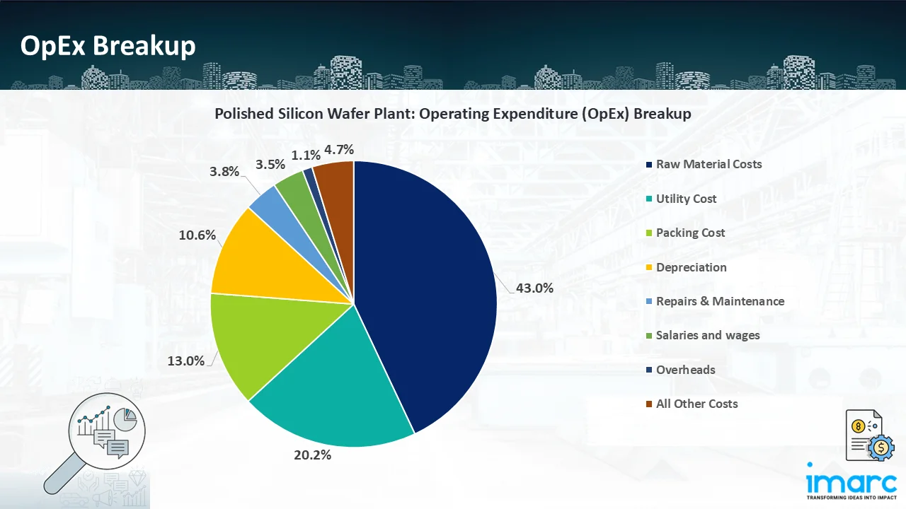
- Operating Expenditure (OpEx): Operating expenditure is the cost incurred to operate a manufacturing plant effectively. Opex in a manufacturing plant typically includes the cost of raw materials, utilities, depreciation, taxes, packing cost, transportation cost, and repairs and maintenance. The operating expenses are part of the cost structure of a manufacturing plant and have a significant effect on profitability and efficiency. Effective control of these costs is necessary for maintaining competitiveness and growth.
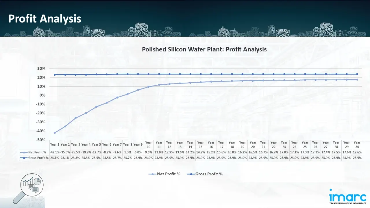
- Profitability Analysis Year on Year Basis: The proposed polished silicon wafer plant, with a capacity of 2,000,000 units of polished silicon wafer annually, achieved an impressive revenue of INR 3.5 billion in its first year. We assisted our client in developing a detailed cost model, which projects steady growth, with revenue rising throughout the projected period. Moreover, gross profit margins improve from 23.1% to 23.9% by year 30, and net profit rises from a negative of 42.1% to a positive of 17.6%, highlighting strong financial viability and profitability.
Conclusion & IMARC's Impact:
Our financial model for the polished silicon wafer manufacturing plant was meticulously developed to meet the client’s objectives, providing an in-depth analysis of production costs, including raw materials, manufacturing, capital expenditure, and operational expenses. By addressing the specific requirements of producing 2,000,000 units of polished silicon wafer annually, we successfully identified key cost drivers and projected profitability, considering market trends, inflation, and potential fluctuations in raw material prices. This comprehensive financial model equipped the client with valuable insights into strategic decision-making, demonstrating our commitment to delivering high-quality, client-focused solutions that ensure the long-term success of large-scale manufacturing ventures.
Latest News and Developments:
- In August 2025, the Indian Union Electronics and IT Minister Ashwini Vaishnaw announced that India is constructing a high-capacity silicon manufacturing unit that can produce 50,000 wafer starts each month. The project, which involves an investment of Rs 91,000 crore and is headed by Tata Electronics in Dholera, Gujarat, was approved by the government in February 2024.
- In May 2025, Taiwanese silicon wafer manufacturer GlobalWafers announced that it would invest an additional $4 billion in the United States to meet growing customer demand there, as it officially opened its new US$ 3.5 billion wafer facility in Texas.
- In October 2024, Infineon pushes technological limits and increases energy efficiency by revealing the thinnest silicon power wafer in the world. Their silicon power wafers, which are produced in a large semiconductor fabrication facility, are only 20 micrometres thick and 300 millimetres in diameter. At just 25% the thickness of a human hair, the ultra-thin silicon wafers are half as thick as the most advanced wafers, which are 40–60 micrometres thick.
Why Choose IMARC:
IMARC's Financial Model Expertise: Helping Our Clients Explore Industry Economics
IMARC is a global market research company that offers a wide range of services, including market entry and expansion, market entry and opportunity assessment, competitive intelligence and benchmarking, procurement research, pricing and cost research, regulatory approvals and licensing, factory setup, factory auditing, company incorporation, incubation services, recruitment services, and marketing and sales.
Under our factory setup services, we assist our clients in exploring the feasibility of their plants by providing comprehensive financial modeling. Additionally, we offer end-to-end consultation for setting up a plant in India or abroad. Our financial modeling includes an analysis of capital expenditure (CapEx) required to establish the manufacturing facility, covering costs such as land acquisition, building infrastructure, purchasing high-tech production equipment, and installation. Furthermore, the layout and design of the factory significantly influence operational efficiency, energy consumption, and labor productivity, all of which impact long-term operational expenditure (OpEx). So, every parameter is covered in the analysis.
At IMARC, we leverage our comprehensive market research expertise to support companies in every aspect of their business journey, from market entry and expansion to operational efficiency and innovation. By integrating our factory setup services with our deep knowledge of industry dynamics, we empower our clients to not only establish manufacturing facilities but also strategically position themselves in highly competitive markets. Our financial modeling and end-to-end consultation services ensure that clients can explore the feasibility of their plant setups while also gaining insights into competitors' strategies, technological advancements, and regulatory landscapes. This holistic approach enables our clients to make informed decisions, optimize their operations, and align with sustainable practices, ultimately driving long-term success and growth.
Our Clients


Contact Us
Have a question or need assistance?
Please complete the form with your inquiry or reach out to us at
Phone Number
+91-120-433-0800+1-201-971-6302
+44-753-714-6104
Previous Post

AI is revolutionizing Japan’s semiconductor industry by boosting innovation and efficiency across the entire value chain. Advanced artificial intelligence (AI)-powered Electronic Design Automation (EDA) tools significantly shorten chip design cycles, improving performance and energy efficiency.
Recent projections indicate that Australia semiconductor market, including services, is growing at a steady compound annual growth rate as the nation deepens its tech infrastructure. The importance of semiconductors spans electronics, defense systems, telecommunications, and emerging AI applications, which position the local ecosystem as strategically vital for growth.
Fiber optic cables are high-tech communications cables that carry information like bursts of light along extremely thin glass or plastic strands, providing high-speed, high-bandwidth connectivity with little loss of signal. Fiber optic cables make up the foundation of contemporary telecommunications, carrying internet, cloud computing, 5G networks, and smart infrastructure.
CAT (Category) cables are twisted-pair Ethernet cables utilized for copper-based wired network communications, varying from CAT5e to CAT8 standards. The cables carry data through copper conductors, but with different speeds (up to 40 Gbps for CAT8) and bandwidths, supporting networks such as LANs, data centers, and smart buildings.
India's semiconductor industry is undergoing a revolutionary phase driven by rising demand from industries like consumer electronics, automotive technologies, industrial automation, and telecom infrastructure.
USB data cables are critical elements of contemporary digital connectivity, enabling high-speed and consistent data transfer and power supply for a broad scope of electronic products. They provide the foundation for charging and synchronizing smartphones, tablets, laptops, and other peripherals, with significant applications in consumer electronics, industrial automation, and new technologies. With technologies like USB-C, the cables today carry faster data speeds, more power output, and universal compatibility, making them essential in a world that is connected.
Thin-film-transistor (TFT) liquid-crystal display (LCD) is a type of display technology used in many electronic devices, such as smartphones, tablets, laptops, and televisions (TVs). A backlight, colour filters, a thin-film transistor array, and a liquid crystal layer are among the layers that make up this flat-panel display. TFT LCDs are made to produce sharp images with superb viewing angles, strong contrast, and accurate colour reproduction. They are made up of thousands of tiny transistors that regulate how much light enters each pixel. This makes it possible for the display to generate crisp, detailed images at rapid refresh rates. TFT LCD technology's low power consumption is one of its main benefits, which makes it perfect for battery-operated gadgets.
Polycrystalline solar photovoltaic (PV) modules are a key component of solar energy systems, harnessing sunlight and converting it into electricity through the photovoltaic effect. These modules are composed of multiple interconnected solar cells, each made from polycrystalline silicon. Polycrystalline solar panels are renowned for their efficiency, affordability, and versatility, making them a popular choice for various applications such as solar installations, commercial and industrial projects, off-grid systems and solar farms.
The LED chip is the core component of an LED bulb, comprising semiconductor layers that enable the free flow of protons and electrons. Employed in all LED lighting fixtures—from bulbs to tubes—the LED chip fundamentally determines light quality, with variations in brightness, voltage, and wavelength. These chips are manufactured through a process called MOCVD (metal-organic chemical vapor deposition), which creates the semiconductor layers that facilitate electric flow. Major applications of these chips include backlighting, illumination, automotive lighting, signs, and signals.
Semiconductors are crucial components in the modern electronics industry, used in electronic equipment and devices to manage and control the flow of electricity. They are found in consumer items like smartphones, wearables, smart TVs, and advanced equipment used in industrial applications, defense, and aerospace. Semiconductors are further divided into four broad categories: optoelectronics, discrete components, integrated circuits, and sensors. Memory devices, logic devices, analog ICs, MPUs, discrete power devices, MCUs, and sensors are some of the major components of semiconductors.