How AI is Transforming the Future of Semiconductors in Japan?
AI is revolutionizing Japan’s semiconductor industry by boosting innovation and efficiency across the entire value chain. Advanced artificial intelligence (AI)-powered Electronic Design Automation (EDA) tools significantly shorten chip design cycles, improving performance and energy efficiency. In manufacturing, AI combined with Internet of Things (IoT) sensors enables predictive maintenance, cutting downtime by up to 50% and extending equipment life. AI-driven robotics enhance automation in packaging and assembly, reducing defects and increasing precision. These improvements raise yield rates and lower costs. Government initiatives and strategic partnerships with private firms and academia fuel continuous AI research and development (R&D), positioning Japan as a global leader in next-generation semiconductor technologies.
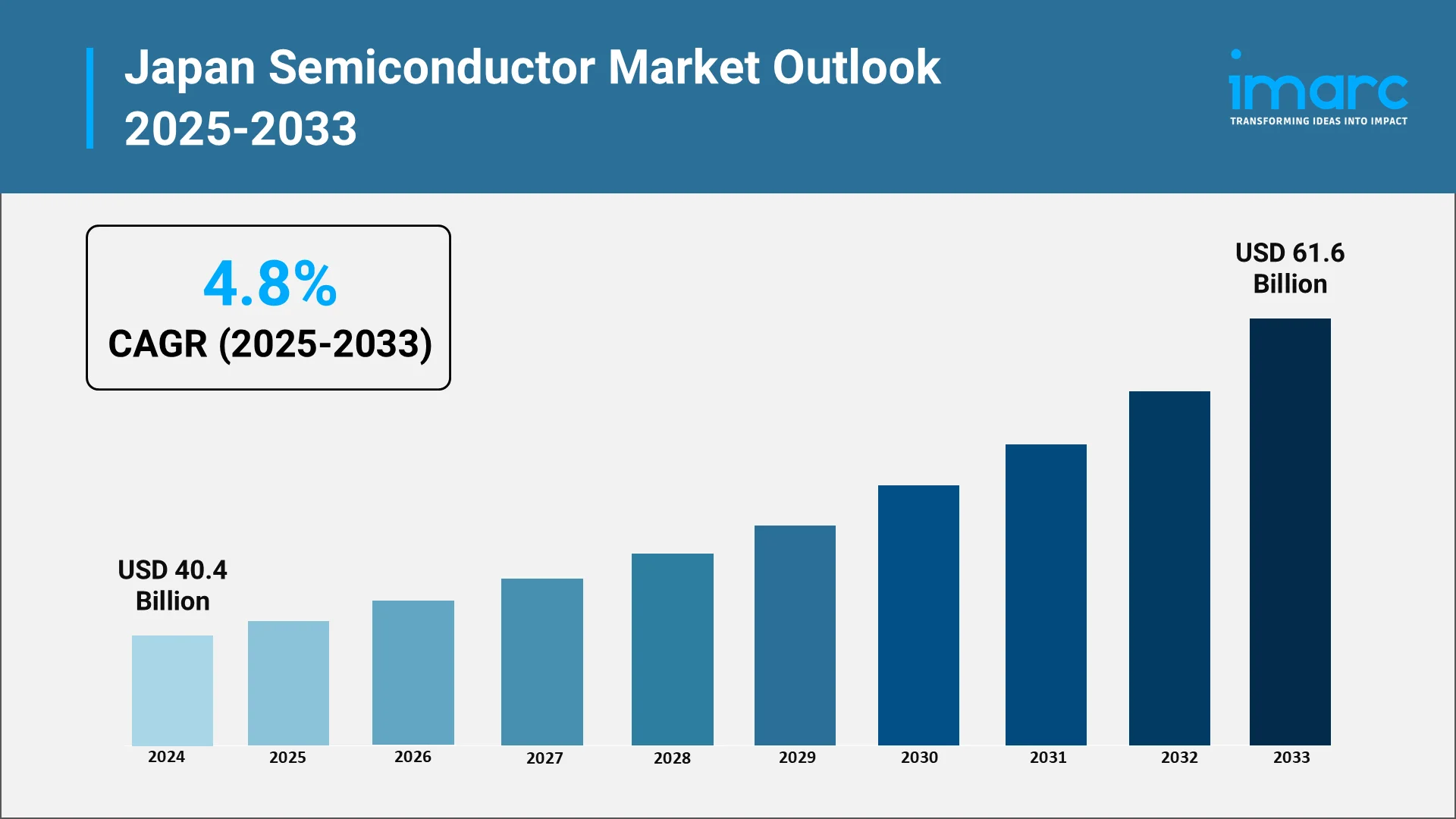
Semiconductors in Japan are experiencing high demand from automotive, consumer electronics, and AI-driven manufacturing sectors. Government initiatives under the “Next-Generation Semiconductor Strategy” are boosting domestic production, attracting investments from global players like TSMC and Micron. Japan’s strength in materials, precision equipment, and advanced packaging supports its competitiveness. Rising adoption of fifth generation (5G), IoT, and electric vehicles (EVs) is fueling innovation, while strategic partnerships and R&D collaborations aim to reduce reliance on imports and strengthen supply chain resilience.
Japan's government unveiled a 2 trillion yen ($13.2 billion) stimulus to boost AI and semiconductor growth, aiming to rebuild domestic capacity and reduce offshore reliance exposed during COVID-19. The plan supports AI-enabled chip development beyond 5nm, attracting investors with medium-term financial incentives. Generative AI could unlock 148.7 trillion yen in productivity, aiding economic growth and societal challenges like an aging population. Regional diversification and shifting public tech perception remain key hurdles.
Explore in-depth findings for this market, Request Sample
AI-Powered Advancements in Japan’s Chip Design Processes:
In Japan’s semiconductor arena, AI is sparking a revolution, turbocharging chip design like never before. Acting as both a visionary artist and master strategist, AI enables engineers to rapidly explore thousands of design possibilities, predicting real-world performance with stunning accuracy. This approach accelerates what once took months into just days, allowing designers to fine-tune architectures that strike the perfect balance between speed, power efficiency, and heat management. Such precision is vital for next-generation logic and memory chips powering AI accelerators, high-performance computing, and sprawling data centers industries where every millisecond and nanometer counts.
Recently, AI-assisted designs have surged from zero to more than half of Japan’s cutting-edge silicon projects. This surge delivers chips with record transistor densities and dramatically reduced power draw fueling devices that are faster, leaner, and more sustainable. By embedding AI deeply into chip design workflows, Japan is crafting a new era of semiconductor innovation, securing a powerful and enduring edge in the fiercely competitive global market. This AI-driven creativity empowers Japanese engineers to push transistor densities to new heights while crafting energy-smart, high-performance semiconductors, redefining the future of chip design.
Smart Manufacturing: AI’s Role in Enhancing Production Efficiency
Inside the Japan semiconductor manufacturing equipment market, factories are becoming intelligent ecosystems. AI quietly orchestrates the workflow monitoring every process, predicting potential faults, and optimizing every machine cycle.
- Predictive maintenance in Japan’s semiconductor manufacturing ensures critical equipment such as wafer etchers and lithography machines is serviced before costly breakdowns occur. Powered by AI and IoT sensors, these systems continuously monitor temperature, vibration, pressure, and other operational parameters in real time. Machine learning algorithms analyze the data to detect subtle patterns that signal early signs of wear or malfunction. By predicting failures before they happen, manufacturers can schedule maintenance during planned downtimes, avoiding unplanned shutdowns, minimizing scrap, and extending equipment life. This proactive approach improves yield rates, optimizes resource use, and keeps Japan’s fabs running at peak efficiency in a highly competitive market.
- In semiconductor fabrication, even the tiniest imperfection can render an entire wafer unusable. AI-driven computer vision now acts as a constant inspector, scanning wafers and components at resolutions far beyond human capability. These systems detect microscopic defects such as pattern misalignments, particle contamination, or minute cracks within milliseconds, preventing flawed chips from advancing through costly production stages. By catching errors early, manufacturers can dramatically cut production waste, lower rework costs, and maintain consistently high yields. This precision not only safeguards profitability but also enhances reliability, ensuring that every chip meets the exacting standards required for high-performance electronics.
- AI-powered process automation is transforming semiconductor manufacturing by fine-tuning operations in real time. From adjusting etch parameters to optimizing thermal processes, these intelligent systems respond instantly to variations, ensuring consistent quality while minimizing waste. In 2023, AI-based process control in fabs delivered a 15% increase in throughput and a 10% reduction in cycle time, directly translating to faster production and lower costs. By reducing material usage and improving energy efficiency, AI not only cuts operational expenses but also supports sustainability goals. This blend of speed, precision, and eco-efficiency positions manufacturers to stay competitive in a rapidly evolving semiconductor landscape.
Industry pioneers such as Renesas, Sony, and Toshiba have turned their fabs into AI-powered production hubs, achieving higher yields, shorter delivery times, and consistently reliable chips. These efficiencies are not just operational advantages—they translate into stronger market positioning and customer trust.
.webp)
Market Dynamics: Investment, R&D, and Export Growth in Japan
AI is powering rapid growth in the Japan semiconductor market, supported by strategic government subsidies, strong private investments, and global partnerships that accelerate innovation. Prime Minister Shigeru Ishiba has unveiled an ambitious plan to invest over ¥10 trillion (about $65 billion) by 2030, highlighting Japan’s dedication to advancing AI technologies. In the semiconductor diode segment, AI is driving breakthroughs in high-frequency and high-power devices critical for electric vehicles, renewable energy systems, and ultra-fast 5G networks. At the same time, AI-led research in advanced materials is strengthening Japan’s position as a global leader in specialized, high-value semiconductor exports. Together, these efforts form a cohesive national strategy aimed at expanding Japan’s share in the global semiconductor market while reducing dependence on foreign suppliers. By integrating AI at every stage, Japan is securing its competitive edge and building a resilient, innovative semiconductor industry for the future.
Japan’s Strategic Roadmap for Semiconductor Resilience with AI:
Japan’s semiconductor roadmap is both ambitious and strategic, focusing on building domestic resilience, scaling AI adoption, and leading in advanced chip technology. This vision aims to reduce reliance on foreign suppliers while positioning Japan as a global leader in semiconductor innovation. By strengthening local capabilities, Japan can better navigate supply chain challenges and foster sustainable growth in this critical industry.
In the semiconductor packaging market, AI is revolutionizing complex processes such as three dimensional (3D) chip stacking, wafer-level integration, and thermal management. These AI-driven advancements improve efficiency, performance, and reliability, enabling the production of smaller, faster, and more energy-efficient chips. Meanwhile, in the foundry sector, AI accelerates prototyping and enhances yield predictability, allowing manufacturers to meet the growing demand for customized chips from international clients.
Collaboration remains central to this transformation. University research labs, corporate R&D centers, and global foundries are forging cross-border alliances to accelerate innovation. By embedding AI at every stage of semiconductor development from design to fabrication Japan establishes a robust pipeline that drives continuous advancement and secures its place at the forefront of the semiconductor industry.
Regional Innovation Hubs: Tokyo, Osaka, and Kyushu
Japan’s AI–semiconductor synergy thrives in its innovation hubs:
- Tokyo: Tokyo stands as Japan’s hub for semiconductor design and AI innovation. It hosts numerous cutting-edge design firms and vibrant AI startups driving breakthroughs in chip architecture and smart technologies. The city also benefits from strong government-backed semiconductor programs that provide funding, policy support, and collaborative opportunities. This synergy fosters a dynamic environment where advanced chip design and AI development converge, fueling innovation and growth in Japan’s semiconductor industry.
- Kyushu: Kyushu, known as “Silicon Island,” is a vital hub for semiconductor manufacturing and research in Japan. Since 2021, it has attracted over 100 semiconductor-related investments totaling around ¥5 trillion ($34 billion), fueling the development of advanced fabrication plants equipped with cutting-edge technology for high-performance chips. The region also hosts leading research institutes that drive semiconductor process innovation through strong collaboration between academia and industry. This dynamic ecosystem ensures Kyushu remains a key player in advancing semiconductor technology, strengthening Japan’s global competitiveness in this critical sector.
- Osaka: Osaka stands as a powerhouse in manufacturing equipment innovation and industrial robotics, crucial for semiconductor fabrication. In 2023, Japan installed 46,106 industrial robots, securing its spot as the world’s second-largest market, just behind China. Osaka leads this charge by developing next-generation machinery and automation technologies that boost production precision, speed, and efficiency. By seamlessly integrating AI into industrial robotics, the city enables smarter, more adaptable manufacturing processes that cut costs and minimize defects. This makes Osaka a vital hub driving Japan’s semiconductor manufacturing capabilities forward on a global scale.
Together, these regions form a collaborative ecosystem that fosters rapid prototyping, knowledge-sharing, and commercialization at scale.
Future Outlook: Challenges and Opportunities Ahead
The future of the Japan semiconductor market holds great promise, yet it faces notable challenges that must be addressed. A critical shortage of AI talent hampers the ability to fully leverage cutting-edge technologies, while the high costs associated with research and development place pressure on companies and government initiatives. Additionally, growing cybersecurity threats pose risks to the integrity of semiconductor design and manufacturing processes, making robust security measures essential.
Despite these obstacles, significant opportunities lie ahead. The Japan semiconductor foundry market is poised for substantial growth as global technology firms increasingly seek reliable, advanced fabrication partners. Japan’s integration of AI-driven efficiencies across the semiconductor value chain—from design and manufacturing to packaging and logistics positions it as a strong contender in the specialized, high-end chip market. This combination of trust, innovation, and efficiency could establish Japan as a preferred supplier worldwide.
If Japan continues to deepen AI integration within its semiconductor ecosystem, it will not just reclaim its historical leadership but will also set new global standards. By aligning technology, talent, and strategy, Japan can redefine the future of the semiconductor industry and secure its position as a global innovation powerhouse.
Insight to Impact: IMARC’s Guide to Transforming Japan’s Semiconductor Industry
IMARC Group empowers semiconductor manufacturers, investors, and policymakers to navigate the Japan Semiconductor Market as artificial intelligence reshapes chip design, manufacturing, and global competitiveness. Our expertise enables stakeholders to harness AI for innovation, operational efficiency, and sustainable growth.
- Market Insights: Explore emerging trends in AI-driven chip architecture, smart manufacturing, predictive maintenance, defect detection, and advanced packaging solutions across Japan’s semiconductor value chain.
- Strategic Forecasting: Anticipate market growth, identify segment-specific opportunities, and assess how AI-powered analytics are expected transform production efficiency, product development, and export strategies.
- Competitive Intelligence: Track leading players, innovative startups, and R&D hubs pioneering AI applications in fabrication, design automation, and semiconductor equipment optimization.
- Policy & Regulatory Analysis: Decode government initiatives, AI-tech partnerships, and national semiconductor resilience strategies shaping the industry’s future.
- Tailored Consulting: Deliver customized strategies for design precision, manufacturing excellence, packaging innovation, and leveraging AI for global market leadership.
As Japan’s semiconductor industry advances in the AI era, IMARC Group stands as a trusted partner—providing actionable insights to help clients unlock new growth avenues and lead in the next generation of chip innovation.
Our Clients


Contact Us
Have a question or need assistance?
Please complete the form with your inquiry or reach out to us at
Phone Number
+91-120-433-0800+1-201-971-6302
+44-753-714-6104
Previous Post

Recent projections indicate that Australia semiconductor market, including services, is growing at a steady compound annual growth rate as the nation deepens its tech infrastructure. The importance of semiconductors spans electronics, defense systems, telecommunications, and emerging AI applications, which position the local ecosystem as strategically vital for growth.
Fiber optic cables are high-tech communications cables that carry information like bursts of light along extremely thin glass or plastic strands, providing high-speed, high-bandwidth connectivity with little loss of signal. Fiber optic cables make up the foundation of contemporary telecommunications, carrying internet, cloud computing, 5G networks, and smart infrastructure.
CAT (Category) cables are twisted-pair Ethernet cables utilized for copper-based wired network communications, varying from CAT5e to CAT8 standards. The cables carry data through copper conductors, but with different speeds (up to 40 Gbps for CAT8) and bandwidths, supporting networks such as LANs, data centers, and smart buildings.
India's semiconductor industry is undergoing a revolutionary phase driven by rising demand from industries like consumer electronics, automotive technologies, industrial automation, and telecom infrastructure.
USB data cables are critical elements of contemporary digital connectivity, enabling high-speed and consistent data transfer and power supply for a broad scope of electronic products. They provide the foundation for charging and synchronizing smartphones, tablets, laptops, and other peripherals, with significant applications in consumer electronics, industrial automation, and new technologies. With technologies like USB-C, the cables today carry faster data speeds, more power output, and universal compatibility, making them essential in a world that is connected.
Thin-film-transistor (TFT) liquid-crystal display (LCD) is a type of display technology used in many electronic devices, such as smartphones, tablets, laptops, and televisions (TVs). A backlight, colour filters, a thin-film transistor array, and a liquid crystal layer are among the layers that make up this flat-panel display. TFT LCDs are made to produce sharp images with superb viewing angles, strong contrast, and accurate colour reproduction. They are made up of thousands of tiny transistors that regulate how much light enters each pixel. This makes it possible for the display to generate crisp, detailed images at rapid refresh rates. TFT LCD technology's low power consumption is one of its main benefits, which makes it perfect for battery-operated gadgets.
Polycrystalline solar photovoltaic (PV) modules are a key component of solar energy systems, harnessing sunlight and converting it into electricity through the photovoltaic effect. These modules are composed of multiple interconnected solar cells, each made from polycrystalline silicon. Polycrystalline solar panels are renowned for their efficiency, affordability, and versatility, making them a popular choice for various applications such as solar installations, commercial and industrial projects, off-grid systems and solar farms.
The LED chip is the core component of an LED bulb, comprising semiconductor layers that enable the free flow of protons and electrons. Employed in all LED lighting fixtures—from bulbs to tubes—the LED chip fundamentally determines light quality, with variations in brightness, voltage, and wavelength. These chips are manufactured through a process called MOCVD (metal-organic chemical vapor deposition), which creates the semiconductor layers that facilitate electric flow. Major applications of these chips include backlighting, illumination, automotive lighting, signs, and signals.
Semiconductors are crucial components in the modern electronics industry, used in electronic equipment and devices to manage and control the flow of electricity. They are found in consumer items like smartphones, wearables, smart TVs, and advanced equipment used in industrial applications, defense, and aerospace. Semiconductors are further divided into four broad categories: optoelectronics, discrete components, integrated circuits, and sensors. Memory devices, logic devices, analog ICs, MPUs, discrete power devices, MCUs, and sensors are some of the major components of semiconductors.