E-Waste Processing Cost Model: From Electronic Scrap to Resource Recovery
_11zon.webp)
What is E-Waste?
E-waste, or electronic waste, is electrical and electronic equipment that has been discarded, such as computers, cell phones, television sets, servers, and household appliances. It is among the world's fastest-growing streams of waste, consisting of a heterogeneous combination of metals, plastics, glass, and toxic substances.
Key Applications Across Industries:
E-waste contains valuable metals like copper, aluminum, gold, silver, palladium, and rare earth elements, in addition to toxic materials like lead, mercury, cadmium, and brominated flame retardants. Treatment of e-waste includes dismantling, sorting, mechanical shredding, and metallurgical or chemical treatments for the recovery of valuable fractions and elimination of hazardous fractions. Most notable properties of e-waste are its high potential for recyclability, high economic value, and environmental hazard if not disposed of properly. The uses of recovered material range from electronics, automotive, energy storage, to construction industries. Benefits of e-waste processing are resource saving, less virgin mining dependency, waste reduction, and environmental regulation compliance. Economically, it fosters circular supply chains and recycling industry job creation. With international sustainability ambitions and increased digitalization, the future for e-waste processing is bright, which translates into increasing demand for sophisticated recycling facilities.
What the Expert Says: Market Overview & Growth Drivers
The global e-waste processing market size reached 20.9 Million MT in 2025. According to IMARC Group, the market is projected to reach 77.4 Million MT by 2034, at a projected CAGR of 15.20% during 2026-2034. The e-waste processing market is influenced by several demand drivers. Increased global consumption of electrical equipment, compounded by short obsolescence cycles, is regularly putting additional volumes into the waste stream.
Increasing regulations, including the EU's Waste Electrical and Electronic Equipment (WEEE) Directive and the E-Waste Management Rules in China, are imposing producer responsibility and recycling requirements. Enhanced demand for key raw materials, including rare earth and precious metals, also stimulates recovery efforts. Urban mining is becoming the most important trend, with e-waste being viewed as a pool of critical materials. In the next five years, digital technology like AI-based sorting, robotic disassembly, and hydrometallurgical procedures will redefine competitive strengths. Challenges, though, are high variability within waste streams, noxious emissions in the course of improper recycling, and control by the informal sector in developing economies. On sustainability, e-waste recycling minimizes landfill charges, reduces CO2 emissions associated with original mining, and facilitates circular economy business models. Industry reaction is in the form of extended producer responsibility (EPR) schemes, international collaborations between electronics companies and recyclers, and funding for sophisticated material recovery technology.
Case Study on Cost Model of E-Waste Processing Plant:
Objective
One of our clients reached out to us to conduct a feasibility study for setting up a medium to large-scale e-waste processing plant.
IMARC Approach: Comprehensive Financial Feasibility
We developed a comprehensive financial model for the setup and operation of a proposed e-waste processing plant in Malaysia. This plant is designed to process 360,000 tons of e-waste annually.
Processing Process: E-waste processing is a step-by-step procedure to extract valuable material with less environmental risk. The process starts with collection and sorting, where e-waste is collected from different sources and sorted into groups such as metals and non-metals for safe disposal. Then, dismantling separates parts such as circuit boards, wires, screens, and batteries, removal of hazardous substances such as mercury or PCBs. They are then reduced in size-by-size reduction (shredding) into smaller uniform pieces, which are easier to process downstream. Magnetic separation is used to recover ferrous metals like steel, while eddy current separation recovers the non-ferrous metals like copper and aluminum. For recovery of high-value materials, the hydrometallurgical process utilizes chemical solutions to dissolve precious and base metals, while pyrometallurgical processing involves high-temperature smelting to extract metals, although less frequently because of energy consumption and emissions. Last, the recovered materials are processed by refining with chemical, electrolytic, or thermal methods to yield pure, marketable metals such as gold, silver, and copper. This combined process not only optimizes resource recovery but also minimizes landfill waste and prevents the release of harmful substances, helping achieve a more circular and sustainable economy.
_11zon.webp)
Get a Tailored Feasibility Report for Your Project Request Sample
Mass Balance and Raw Material Required: The primary raw materials used in the e-waste processing plant is e-waste. For a plant processing 1 ton of e-waste, final products include 0.11 ton of copper, 0.60 ton of ferrous metals, 0.08 ton of aluminum and 0.003 ton of other precious metal.
Machineries Required:
- 1000 type belt conveyor platform
- Dust Hoods, Dust Pipes and Exhaust Duct
- Dust Collector
- 1200 belt trough conveyor
- 1800 double shaft intelligent shredder Working chamber : 1 8 00 × 1 206 m
- 800 type z type conveyor
- Dust hood with duct fittings
- R ES - 1 50 0 hammer impact crusher with bottom discharger
- 1 2 00 cyclone feeder
- 128 type pulse dust collector ( 128 bags )
- 800 linear vibrating screen
- 800 Drum Magnetic Separator
- 1-750 Baffled Air Separator
- 1 2 00 cyclone feeder
- Type 96 Pulse Dust Collector
- 800 Conveyor
- 600 Suspension Magnetic Separator
- R ES - 1000 Eddy Current Separator
- 600 Belt Conveyor
- Comprehensive exhaust duct support pipe fittings and other systems
- PLC control cabinet
- Electronic component disassembly machine
- Flue gas purification system
- Multi-layer vibrating screen
- Magnetic Separator
- PCB Component Dismantling Machine
- TC-50 Carbonization Furnace
- 5 Layer Separation Screener
- Magnetic Separator
- Vibrating Screen
- BC-100 Ball Crusher
- 500L Reactor
- 500L Reactor
- 800L Reactor
- G800 Vacuum Filter Disc
- C500 Vacuum Storage Tank
- PL1200 Spray Tower
- ZKP-5 Vacuum Pump
- Precious Metal Working Platform
- GX-1500 High Temperature Circulation Tank
- PF-800 Liquid Tank
- 32FSB Acid Resistant Pump
- PY-500 Medicament Storage Tank
- PY-1000 Water Tank
- PYJ-500 Metering Tank
- CQ50-4 Extractor
- Acid Gas Absorption
- 50L Reactor
- GX-100 High Temperature Circulating Tank
- GL-20 Filter
- ZKP-2 Vacuum Pump
- Electric control cabinet
- Others
Techno-Commercial Parameter:
- Capital Investment (CapEx): Capital expenditure (CapEx) in a Processing plant includes various investments essential for its setup and long-term operations. It covers machinery and equipment costs, including procurement, installation, and commissioning. Civil works expenses involve land development, factory construction, and infrastructure setup. Utilities such as power, water supply, and HVAC systems are also significant. Additionally, material handling systems, automation, environmental compliance, and safety measures are key components. Other expenditures include IT infrastructure, security systems, and office essentials, ensuring operational efficiency and business growth.
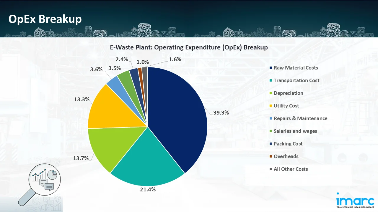
- Operating Expenditure (OpEx): Operating expenditure is the cost incurred to operate a Processing plant effectively. Opex in a Processing plant typically includes the cost of raw materials, utilities, depreciation, taxes, packing cost, transportation cost, and repairs and maintenance. The operating expenses are part of the cost structure of a Processing plant and have a significant effect on profitability and efficiency. Effective control of these costs is necessary for maintaining competitiveness and growth.
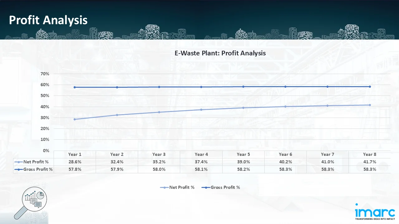
- Profitability Analysis Year on Year Basis: The proposed e-waste processing plant, with a capacity of processing 360,000 tons of e-waste annually, achieved an impressive revenue of USD 77.8 million in its first year. We assisted our client in developing a detailed cost model, which projects steady growth, with revenue rising throughout the projected period. Moreover, gross profit margins improve from 57.8% to 58.3% by year 8, and net profit rises from 28.6% to 41.7%, highlighting strong financial viability and profitability.
Conclusion & IMARC's Impact:
Our financial model for the e-waste processing plant was meticulously developed to meet the client’s objectives, providing an in-depth analysis of production costs, including raw materials, processing, capital expenditure, and operational expenses. By addressing the specific requirements of processing 360,000 tons of e-waste annually, we successfully identified key cost drivers and projected profitability, considering market trends, inflation, and potential fluctuations in raw material prices. This comprehensive financial model equipped the client with valuable insights into strategic decision-making, demonstrating our commitment to delivering high-quality, client-focused solutions that ensure the long-term success of large-scale Processing ventures.
Latest News and Developments:
- In August 2025, Government of Delhi announced preparing to construct one of the most sophisticated e-waste processing plants in India, drawing inspiration from Norway's innovative approach. The proposed Holambi Kalan facility in North Delhi will have an almost low environmental impact and be able to handle double its initial capacity.
- In October 2024, to provide a more sustainable supply of the precious metal for the coin manufacturer's high-end jewellery line, the Royal Mint has opened a "pioneering" operation that will recover gold from technological waste. The south Wales facility, which has been in operation since March 2022, is intended to extract gold from up to 4,000 tonnes of circuit boards per year that are sourced from gadgets such as TVs, computers, and phones that are made in the UK.
- In August 2024, the first alkaline battery recycling facility has been opened by ERI, which has its headquarters in Fresno, California. The plant, according to the cybersecurity-focused hardware destruction and information technology asset disposal (ITAD) company, is located inside its current 315,000-square-foot electronics recycling and ITAD facility in Plainfield, Indiana.
Why Choose IMARC:
IMARC's Financial Model Expertise: Helping Our Clients Explore Industry Economics
IMARC is a global market research company that offers a wide range of services, including market entry and expansion, market entry and opportunity assessment, competitive intelligence and benchmarking, procurement research, pricing and cost research, regulatory approvals and licensing, factory setup, factory auditing, company incorporation, incubation services, recruitment services, and marketing and sales.
Under our factory setup services, we assist our clients in exploring the feasibility of their plants by providing comprehensive financial modeling. Additionally, we offer end-to-end consultation for setting up a plant in India or abroad. Our financial modeling includes an analysis of capital expenditure (CapEx) required to establish the Processing facility, covering costs such as land acquisition, building infrastructure, purchasing high-tech production equipment, and installation. Furthermore, the layout and design of the factory significantly influence operational efficiency, energy consumption, and labor productivity, all of which impact long-term operational expenditure (OpEx). So, every parameter is covered in the analysis.
At IMARC, we leverage our comprehensive market research expertise to support companies in every aspect of their business journey, from market entry and expansion to operational efficiency and innovation. By integrating our factory setup services with our deep knowledge of industry dynamics, we empower our clients to not only establish Processing facilities but also strategically position themselves in highly competitive markets. Our financial modeling and end-to-end consultation services ensure that clients can explore the feasibility of their plant setups while also gaining insights into competitors' strategies, technological advancements, and regulatory landscapes. This holistic approach enables our clients to make informed decisions, optimize their operations, and align with sustainable practices, ultimately driving long-term success and growth.
Our Clients


Contact Us
Have a question or need assistance?
Please complete the form with your inquiry or reach out to us at
Phone Number
+91-120-433-0800+1-201-971-6302
+44-753-714-6104
Previous Post

Polished silicon wafers are very pure, ultra-flat semiconductor substrates that are produced from high-quality single-crystal silicon. The wafers act as the material base for making integrated circuits, power devices, and MEMS (Microelectromechanical Systems). The wafers are made of monocrystalline silicon ingots using the Czochralski or Float-Zone process, from which the wafers are cut, lapped, etched, and polished to atomic-scale flatness and defect-free surfaces.
AI is revolutionizing Japan’s semiconductor industry by boosting innovation and efficiency across the entire value chain. Advanced artificial intelligence (AI)-powered Electronic Design Automation (EDA) tools significantly shorten chip design cycles, improving performance and energy efficiency.
Recent projections indicate that Australia semiconductor market, including services, is growing at a steady compound annual growth rate as the nation deepens its tech infrastructure. The importance of semiconductors spans electronics, defense systems, telecommunications, and emerging AI applications, which position the local ecosystem as strategically vital for growth.
Fiber optic cables are high-tech communications cables that carry information like bursts of light along extremely thin glass or plastic strands, providing high-speed, high-bandwidth connectivity with little loss of signal. Fiber optic cables make up the foundation of contemporary telecommunications, carrying internet, cloud computing, 5G networks, and smart infrastructure.
CAT (Category) cables are twisted-pair Ethernet cables utilized for copper-based wired network communications, varying from CAT5e to CAT8 standards. The cables carry data through copper conductors, but with different speeds (up to 40 Gbps for CAT8) and bandwidths, supporting networks such as LANs, data centers, and smart buildings.
India's semiconductor industry is undergoing a revolutionary phase driven by rising demand from industries like consumer electronics, automotive technologies, industrial automation, and telecom infrastructure.
USB data cables are critical elements of contemporary digital connectivity, enabling high-speed and consistent data transfer and power supply for a broad scope of electronic products. They provide the foundation for charging and synchronizing smartphones, tablets, laptops, and other peripherals, with significant applications in consumer electronics, industrial automation, and new technologies. With technologies like USB-C, the cables today carry faster data speeds, more power output, and universal compatibility, making them essential in a world that is connected.
Thin-film-transistor (TFT) liquid-crystal display (LCD) is a type of display technology used in many electronic devices, such as smartphones, tablets, laptops, and televisions (TVs). A backlight, colour filters, a thin-film transistor array, and a liquid crystal layer are among the layers that make up this flat-panel display. TFT LCDs are made to produce sharp images with superb viewing angles, strong contrast, and accurate colour reproduction. They are made up of thousands of tiny transistors that regulate how much light enters each pixel. This makes it possible for the display to generate crisp, detailed images at rapid refresh rates. TFT LCD technology's low power consumption is one of its main benefits, which makes it perfect for battery-operated gadgets.
Polycrystalline solar photovoltaic (PV) modules are a key component of solar energy systems, harnessing sunlight and converting it into electricity through the photovoltaic effect. These modules are composed of multiple interconnected solar cells, each made from polycrystalline silicon. Polycrystalline solar panels are renowned for their efficiency, affordability, and versatility, making them a popular choice for various applications such as solar installations, commercial and industrial projects, off-grid systems and solar farms.
The LED chip is the core component of an LED bulb, comprising semiconductor layers that enable the free flow of protons and electrons. Employed in all LED lighting fixtures—from bulbs to tubes—the LED chip fundamentally determines light quality, with variations in brightness, voltage, and wavelength. These chips are manufactured through a process called MOCVD (metal-organic chemical vapor deposition), which creates the semiconductor layers that facilitate electric flow. Major applications of these chips include backlighting, illumination, automotive lighting, signs, and signals.
Semiconductors are crucial components in the modern electronics industry, used in electronic equipment and devices to manage and control the flow of electricity. They are found in consumer items like smartphones, wearables, smart TVs, and advanced equipment used in industrial applications, defense, and aerospace. Semiconductors are further divided into four broad categories: optoelectronics, discrete components, integrated circuits, and sensors. Memory devices, logic devices, analog ICs, MPUs, discrete power devices, MCUs, and sensors are some of the major components of semiconductors.