Top Factors Driving Growth in Japan's Printed Circuit Board Industry
Introduction: The Rising Importance of PCBs in Japan’s High-Tech Landscape
Japan's printed circuit board (PCB) industry is the world leader in technology innovation, enabling consumer electronics, automotive, and next-generation communication system development. As a key enabler of modern electronic products, PCBs provide the essential building blocks for embedding semiconductors, sensors, and microchips into miniaturized, high-performance devices. Japan, through its world-class manufacturing base and engineering expertise, remains the hub of the global PCB supply chain.
The industry has picked up speed as a result of the country's strong electronics ecosystem, tech R&D efforts, and value-added manufacturing government initiative. For instance, industry reports show that in January 2024, Japanese production of electronic products was 322,198 units, which equates to a production index of 111.0 percent. This growth validates the country's manufacturing strength and tech capabilities. In particular, Japan's emphasis on miniaturization, precision engineering, and quality control has established it as a global leader in producing complex rigid, flexible, and HDI (high-density interconnect) boards. The expanding application of high-performance PCBs from smartphones to electric vehicles suggests the direction the industry is taking. With the mass adoption of 5G, IoT, and AI technologies, the Japanese PCB market will keep expanding in the decade to come.
Explore in-depth findings for this market, Request Sample
Consumer Electronics Boom: Fueling PCB Growth in Japan
Consumer electronics remain the prime catalyst of PCB demand in Japan, fueled by the nation's leadership in innovation and manufacturing. In May 2024, as per an industry report, production value for PCBs of consumer electronics in Japan rose by 96.3% from year to year. The sharp rise reflects the industry's robust growth.
Japanese companies have been world leaders in electronics, ranging from compact TVs and music centers to advanced gaming consoles and high-speed smartphones. Now, with consumers seeking thinner, more powerful, and power-saving devices, the application of PCBs has also become all the more necessary. HDI (high-density interconnect) PCBs and FPCBs (flexible printed circuit boards) find extensive use in smartphones, tablets, and wearables due to their miniaturization and higher connectivity. Industry estimates point to the fact that Japan's smartphone penetration will exceed 94% of the population by the year 2027, reaching as high as approximately 115.5 Million subscribers. The increased adoption is expected to directly stimulate larger PCB demand.
Furthermore, the introduction of next-generation display technologies such as OLED and micro-LED has also raised the demand for advanced PCB integration to facilitate optimal device performance. Along with this, the expansion of networked appliances and smart home technology showcases the need for reliable, miniaturized PCB solutions. Japan's consumer electronics industry, underpinned by robust domestic production and substantial investment, is driving this growth trajectory. As per industry reports, around USD 101.05 Billion worth of electrical and electronic equipment was exported from Japan in 2024, reflecting the sector's influence worldwide. With exports increasing steadily, PCBs remain an integral part of enhancing product competitiveness and quality. Such steady demand from consumer electronics can be relied upon to support the industry while laying the groundwork for innovation within allied industries like automotive and healthcare.
5G and IoT: The Twin Engines Driving PCB Innovation
5G Rollout Sparks Demand for High-Performance PCBs
The rollout of 5G networks across Japan is significantly boosting the demand for advanced PCBs capable of supporting high-frequency, low-latency communications. Data from the Japanese Ministry of Internal Affairs and Communications indicates that in December 2024, the number of licensees for the 4.7 GHz band had increased to 153, while the 28 GHz band had 25 licensees. Unlike traditional PCBs, those used in 5G infrastructure must handle higher data transmission speeds and complex circuitry for base stations, routers, and small-cell networks. This requires boards with low dielectric loss, high thermal stability, and advanced material engineering. Japanese PCB manufacturers are investing in cutting-edge technologies such as multilayer and high-frequency substrates to meet these requirements. The transition to 5G-enabled smartphones and devices further amplifies demand, making PCBs a cornerstone of the digital transformation.
IoT Revolution Demands Smarter, Smaller, and Flexible PCBs
Parallel to 5G, the expansion of the Internet of Things (IoT) ecosystem is reshaping PCB design requirements in Japan. According to industry reports, the Japan internet of things market size is expected to reach USD 1,86,064.6 Million by 2033, exhibiting a growth rate (CAGR) of 13.30% during 2025-2033. Smart factories, healthcare wearables, logistics sensors, and connected vehicles demand compact yet highly efficient boards. The surge in IoT devices—estimated to reach Billions globally, requires PCBs with flexible architecture, energy efficiency, and durability. Japanese firms, known for their expertise in precision engineering, are innovating with rigid-flex boards and system-in-package (SiP) solutions to address these needs. The seamless integration of PCBs into IoT applications not only drives volume growth but also enhances Japan’s leadership in supplying reliable, future-ready solutions to global markets.
.webp)
Mobility Transformation: How Automotives and EVs Boost PCB Adoption
Next-Gen Vehicles Run on PCB-Powered Electronics
The automotive sector is a critical growth driver for Japan’s PCB industry, with electronic content in vehicles rising exponentially. Additionally, Japan’s carbon neutrality goal for 2050 and government-led plans to electrify the country’s transportation sector are further fueling PCB demand. Modern vehicles rely on PCBs for applications such as infotainment systems, advanced driver-assistance systems (ADAS), digital dashboards, and connectivity modules.
As Japan’s automotive industry is globally renowned for innovation and scale, the demand for reliable, high-quality PCBs is intensifying. Manufacturers are focusing on producing boards with superior thermal management and vibration resistance to ensure performance under harsh automotive environments.
EV Surge Accelerates Innovation in High-Power PCBs
Electric vehicles (EVs) are amplifying this demand further by requiring specialized PCBs for battery management systems, power electronics, and charging infrastructure. Lightweight yet durable boards are critical to ensuring energy efficiency and safety in EV applications. With Japan investing heavily in EV manufacturing and charging networks, the need for advanced multilayer and high-power PCBs is expanding. For instance, in September 2024, the Japanese government allocated JPY 55.7 Billion (USD 391.36 Million) to support Nissan Motor Co. Ltd.’s EV battery research strategy, providing state assistance through financial grants. This initiative reflects Japan’s commitment to advancing EV technology. In response, companies are integrating wide-bandgap semiconductors with PCBs to enhance efficiency and durability in EV systems. This intersection of automotive and PCB innovation positions Japan as a leader in developing next-generation mobility solutions, accelerating the industry’s long-term growth.
Miniaturization and Semiconductors: Advancements Shaping the Future of PCBs
Japan’s expertise in semiconductors and miniaturization is reinforcing the growth of its PCB industry. As consumer and industrial devices become smaller and more powerful, PCBs must accommodate complex circuitry in limited space while maintaining performance. High-density interconnect (HDI) boards, microvia technology, and embedded component PCBs are increasingly being adopted to meet these requirements.
Moreover, the synergy between Japan’s semiconductor industry and PCB manufacturing enhances innovation in packaging solutions, enabling greater speed, heat dissipation, and energy efficiency. Flexible PCBs are also benefiting from these advancements, supporting foldable devices and next-generation medical wearables. With semiconductor miniaturization advancing toward sub-5nm nodes, Japan’s PCB manufacturers are investing in R&D to align with these evolving requirements.
A recent example of this innovation occurred in July 2025, when OKI Circuit Technology announced the launch of rigid-flex PCBs embedded with copper coins, with commercial sales scheduled to begin in August 2025. These advanced boards are designed to enhance heat dissipation in vacuum environments, such as rockets and satellite equipment, while combining rigid and flexible structures to eliminate connectors. This not only saves space and reduces weight but also streamlines assembly, reflecting how Japanese firms are aligning with global demands for miniaturization and advanced engineering.
Future Horizons: Growth Trajectory of Japan’s PCB Market
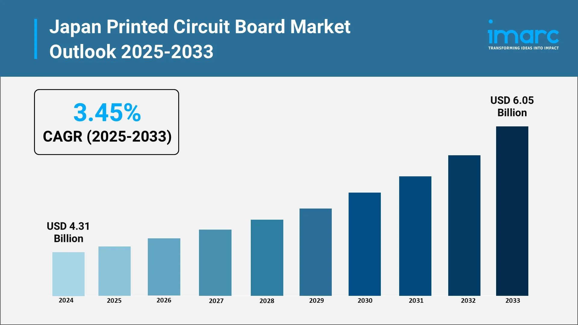
The future of Japan’s PCB industry is defined by sustained demand across electronics, automotive, and communication ecosystems. According to the IMARC Group report, the Japan PCB components market size is expected to reach USD 4,335.95 Million by 2033, exhibiting a growth rate (CAGR) of 11.26% during 2025-2033. With global supply chains shifting toward resilience and regional specialization, Japan’s reputation for precision and quality places it at a competitive advantage. Therefore, the PCB market in Japan is expected to expand steadily as 5G, IoT, EVs, and semiconductor innovation converge.
Key Growth Drivers:
- Rising consumer electronics demand for smartphones, wearables, and smart home devices
- 5G deployment and IoT expansion requiring high-frequency, compact PCBs
- Automotive and EV sector growth fueling demand for durable, high-performance boards
- Semiconductor miniaturization advancing HDI and flexible PCB innovation
- Global supply chain resilience strategies reinforcing Japan’s role as a trusted supplier
Strategic Support: IMARC’s Intelligence for Japan PCB Industry Transformation
As Japan’s printed circuit board (PCB) industry enters a high-growth phase, IMARC Group equips manufacturers, technology providers, investors, and policymakers with actionable insights and strategic intelligence. The convergence of 5G, IoT, automotive electronics, and semiconductor miniaturization is creating unprecedented opportunities for innovation, market expansion, and global competitiveness.
How IMARC Delivers Strategic Value:
- Technology Innovation Mapping: Tracks breakthroughs in HDI, flexible, and high-frequency PCBs that are redefining performance standards across electronics, automotive, and communication sectors.
- Market Penetration Analysis: Evaluates adoption patterns across consumer electronics, EV applications, and IoT ecosystems to optimize product positioning and technology deployment strategies.
- Regulatory Compliance Intelligence: Monitors evolving Japanese and international quality standards, safety protocols, and environmental regulations to ensure compliance while capturing emerging opportunities.
- Competitive Ecosystem Assessment: Profiles leading PCB manufacturers, regional innovators, and global players active in Japan, offering benchmarking insights on capabilities, partnerships, and market positioning.
- Investment Opportunity Identification: Assesses funding trends, R&D initiatives, and government incentives in electronics and PCB manufacturing to guide strategic partnerships and capital allocation.
- Future Market Forecasting: Provides detailed forecasts by PCB type, technology component, end-user sector, and regional market, supporting long-term planning and resilient growth strategies.
Our Clients


Contact Us
Have a question or need assistance?
Please complete the form with your inquiry or reach out to us at
Phone Number
+91-120-433-0800+1-201-971-6302
+44-753-714-6104
Previous Post

Aluminum-Air (Al-Air) battery is a new energy storage technology that has attracted interest as a future alternative to conventional lithium-ion batteries, specifically for electric vehicle (EV) use. As opposed to normal rechargeable batteries, the Al-Air battery is a metal-air electrochemical cell with aluminum as the anode, oxygen from the ambient air as the cathode reactant, and a liquid electrolyte (commonly sodium hydroxide or potassium hydroxide) as the medium through which the reaction occurs.
Aluminium wire is an essential industrial commodity commonly employed in power transmission, electrical distribution, building construction, and manufacturing processes owing to its high conductivity-to-weight ratio, resistance to corrosion, and cost advantage over copper. Produced by methods including continuous casting, rolling, and drawing, aluminum wire is available in various grades and alloys to serve the wide demands, from overhead transmission conductors and building wiring to automotive harnesses and electronic applications.
Air conditioners are electromechanical devices used to control indoor climate by extracting heat and humidity and ensuring optimum air circulation. Generally consisting of a compressor, condenser, evaporator, refrigerant fluid, filters, fans, and electronic controls, air conditioners work based on the principle of heat exchange, moving heat from indoor areas to the external environment. Contemporary units come in diverse configurations, such as split systems, window units, central air systems, and portable models, supporting respective residential, commercial, and industrial applications. Some of the major characteristics are efficiency in cooling, energy use, noise rating, and environmental footprint in relation to refrigerant type.
E-waste, or electronic waste, is electrical and electronic equipment that has been discarded, such as computers, cell phones, television sets, servers, and household appliances. It is among the world's fastest-growing streams of waste, consisting of a heterogeneous combination of metals, plastics, glass, and toxic substances. E-waste contains valuable metals like copper, aluminum, gold, silver, palladium, and rare earth elements, in addition to toxic materials like lead, mercury, cadmium, and brominated flame retardants.
Polished silicon wafers are very pure, ultra-flat semiconductor substrates that are produced from high-quality single-crystal silicon. The wafers act as the material base for making integrated circuits, power devices, and MEMS (Microelectromechanical Systems). The wafers are made of monocrystalline silicon ingots using the Czochralski or Float-Zone process, from which the wafers are cut, lapped, etched, and polished to atomic-scale flatness and defect-free surfaces.
AI is revolutionizing Japan’s semiconductor industry by boosting innovation and efficiency across the entire value chain. Advanced artificial intelligence (AI)-powered Electronic Design Automation (EDA) tools significantly shorten chip design cycles, improving performance and energy efficiency.
Recent projections indicate that Australia semiconductor market, including services, is growing at a steady compound annual growth rate as the nation deepens its tech infrastructure. The importance of semiconductors spans electronics, defense systems, telecommunications, and emerging AI applications, which position the local ecosystem as strategically vital for growth.
Fiber optic cables are high-tech communications cables that carry information like bursts of light along extremely thin glass or plastic strands, providing high-speed, high-bandwidth connectivity with little loss of signal. Fiber optic cables make up the foundation of contemporary telecommunications, carrying internet, cloud computing, 5G networks, and smart infrastructure.
CAT (Category) cables are twisted-pair Ethernet cables utilized for copper-based wired network communications, varying from CAT5e to CAT8 standards. The cables carry data through copper conductors, but with different speeds (up to 40 Gbps for CAT8) and bandwidths, supporting networks such as LANs, data centers, and smart buildings.
India's semiconductor industry is undergoing a revolutionary phase driven by rising demand from industries like consumer electronics, automotive technologies, industrial automation, and telecom infrastructure.
USB data cables are critical elements of contemporary digital connectivity, enabling high-speed and consistent data transfer and power supply for a broad scope of electronic products. They provide the foundation for charging and synchronizing smartphones, tablets, laptops, and other peripherals, with significant applications in consumer electronics, industrial automation, and new technologies. With technologies like USB-C, the cables today carry faster data speeds, more power output, and universal compatibility, making them essential in a world that is connected.
Thin-film-transistor (TFT) liquid-crystal display (LCD) is a type of display technology used in many electronic devices, such as smartphones, tablets, laptops, and televisions (TVs). A backlight, colour filters, a thin-film transistor array, and a liquid crystal layer are among the layers that make up this flat-panel display. TFT LCDs are made to produce sharp images with superb viewing angles, strong contrast, and accurate colour reproduction. They are made up of thousands of tiny transistors that regulate how much light enters each pixel. This makes it possible for the display to generate crisp, detailed images at rapid refresh rates. TFT LCD technology's low power consumption is one of its main benefits, which makes it perfect for battery-operated gadgets.
Polycrystalline solar photovoltaic (PV) modules are a key component of solar energy systems, harnessing sunlight and converting it into electricity through the photovoltaic effect. These modules are composed of multiple interconnected solar cells, each made from polycrystalline silicon. Polycrystalline solar panels are renowned for their efficiency, affordability, and versatility, making them a popular choice for various applications such as solar installations, commercial and industrial projects, off-grid systems and solar farms.
The LED chip is the core component of an LED bulb, comprising semiconductor layers that enable the free flow of protons and electrons. Employed in all LED lighting fixtures—from bulbs to tubes—the LED chip fundamentally determines light quality, with variations in brightness, voltage, and wavelength. These chips are manufactured through a process called MOCVD (metal-organic chemical vapor deposition), which creates the semiconductor layers that facilitate electric flow. Major applications of these chips include backlighting, illumination, automotive lighting, signs, and signals.
Semiconductors are crucial components in the modern electronics industry, used in electronic equipment and devices to manage and control the flow of electricity. They are found in consumer items like smartphones, wearables, smart TVs, and advanced equipment used in industrial applications, defense, and aerospace. Semiconductors are further divided into four broad categories: optoelectronics, discrete components, integrated circuits, and sensors. Memory devices, logic devices, analog ICs, MPUs, discrete power devices, MCUs, and sensors are some of the major components of semiconductors.