Semiconductor Manufacturing Cost Analysis: From Wafer to Wealth
What is Semiconductor?
Semiconductor manufacturing is a highly specialized industrial process that involves the design, fabrication, and assembly of semiconductor devices including integrated circuits (ICs), memory chips, sensors, and discrete components. The process transforms raw semiconductor materials, primarily silicon, into sophisticated electronic components through a combination of physical and chemical processing steps, such as wafer fabrication, photolithography, doping, etching, thin-film deposition, and packaging. Characterized by extreme precision and nanoscale control, semiconductor manufacturing takes place in cleanroom environments equipped with advanced automation, robotics, and process monitoring systems. Each step is designed to ensure defect-free production and high yield rates. The resulting semiconductor devices form the core of modern electronics, powering everything from consumer gadgets to industrial systems and global communications infrastructure.
Key Applications Across Industries:
Semiconductors are at the heart of virtually every modern technology, supporting a broad spectrum of applications across consumer, industrial, and infrastructure domains. In consumer electronics, semiconductors enable the performance and functionality of smartphones, laptops, tablets, televisions, gaming consoles, and wearable devices. They provide essential capabilities for processing, memory storage, connectivity, display control, and power management, making them integral to device efficiency and user experience.
In computing and data infrastructure, semiconductors power servers, networking equipment, and data centers that support cloud computing, artificial intelligence (AI), and high-performance computing (HPC). Advanced processors, GPUs, and memory chips handle the immense data processing demands of modern applications. Similarly, telecommunications systems including 5G base stations, routers, and optical communication networks depend on semiconductors for fast, reliable data transmission.
The automotive industry represents a rapidly growing segment. Semiconductors are key components in engine control units (ECUs), advanced driver-assistance systems (ADAS), battery management systems (BMS), infotainment modules, and electric vehicle (EV) power electronics. As vehicles become more autonomous and electrified, semiconductor usage per vehicle continues to increase significantly.
In industrial and manufacturing sectors, semiconductors are used in automation systems, robotics, sensors, programmable logic controllers (PLCs), and Industrial Internet of Things (IIoT) applications, providing real-time monitoring and precision control. The healthcare and life sciences industries also rely on semiconductor-based devices for medical imaging systems, diagnostic instruments, monitoring equipment, and wearable health sensors. Meanwhile, in energy and utilities, semiconductors enable smart grids, renewable energy inverters, and power management systems, supporting the global transition to cleaner energy.
Finally, aerospace, defense, and security sectors depend on semiconductors for navigation, radar, communication, and surveillance systems, where performance, reliability, and ruggedness are critical. Across these diverse fields, semiconductors remain the foundation of digital innovation and technological progress.
What the Expert Says: Market Overview & Growth Drivers
The global semiconductor market reached a value of USD 739.0 Billion in 2025. According to IMARC Group, the market is projected to reach USD 1,265.2 Billion by 2034, at a projected CAGR of 5.97% during 2026-2034. The global semiconductor manufacturing industry continues to grow rapidly, propelled by digital transformation, technological advancement, and expanding end-use demand.
A major driver is the rising need for computing power and data processing in applications such as AI, machine learning, cloud computing, and big data analytics. These technologies require high-performance logic and memory chips with enhanced processing speed, energy efficiency, and integration density, driving continuous investment in next-generation fabrication nodes and manufacturing capacity. The consumer electronics sector remains a cornerstone of demand. The proliferation of smart and connected devices, coupled with shorter product cycles and rapid innovation, fuels the need for advanced semiconductor components and more efficient production technologies.
Automotive electrification and automation are among the most transformative market forces. Electric vehicles (EVs), autonomous driving systems, and connected car technologies require significantly more semiconductors per vehicle, particularly in power electronics, sensors, microcontrollers, and safety systems. This shift is driving new investment in automotive grade fabs and specialized manufacturing processes. Industrial automation and smart infrastructure further contribute to growth, as industries adopt Industry 4.0 technologies, intelligent sensors, and connected energy systems. Governments around the world are also prioritizing semiconductor self-sufficiency and supply chain resilience, encouraging new fabrication plants (fabs) and R&D investments through policy incentives.
Technological innovation remains a cornerstone of market expansion. Advancements in wafer fabrication, extreme ultraviolet (EUV) lithography, heterogeneous integration, and advanced packaging are enabling more powerful and energy-efficient chips. These developments open new opportunities in AI, edge computing, quantum computing, and next-generation telecommunications (6G).
In summary, the global semiconductor manufacturing industry is being driven by digitalization, electrification, smart infrastructure, and policy support. With its critical role in enabling modern technology, semiconductor manufacturing remains one of the most strategically important and innovation-intensive industries in the world.

Case Study on Cost Model of Semiconductor Manufacturing Plant:
Objective
One of our clients reached out to us to conduct a feasibility study for setting up a medium scale semiconductor manufacturing plant.
IMARC Approach: Comprehensive Financial Feasibility
We developed a comprehensive financial model for the setup and operation of a proposed semiconductor manufacturing plant in India. This plant is designed to manufacture 240,000 wafers of semiconductor annually.
Manufacturing Process: The semiconductor manufacturing process is a highly intricate, multi-stage operation that transforms raw silicon into functional electronic devices with nanoscale precision. It combines advanced materials science, photolithography, and automated engineering systems under extremely controlled conditions to achieve the density, performance, and reliability required by modern electronics. The process begins with the production of ultra-pure silicon ingots, typically grown using the Czochralski or float-zone method to form single-crystal structures. These ingots are sliced into thin wafers using precision diamond saws and then polished to an atomically smooth, defect-free finish. This creates the substrate upon which integrated circuits (ICs) are built. All subsequent fabrication occurs in cleanroom environments, where air purity, temperature, and humidity are tightly controlled to prevent microscopic contamination.
The core of device fabrication lies in photolithography, a patterning technique that defines the intricate circuit layout. A light-sensitive photoresist is applied to the wafer surface and exposed to ultraviolet (UV) or extreme ultraviolet (EUV) light through a photomask containing the circuit design. After exposure and development, specific areas of the wafer are protected or exposed for further processing.
Next, etching processes, either wet chemical or dry plasma etching, remove unwanted material, while deposition techniques such as chemical vapor deposition (CVD), physical vapor deposition (PVD), or atomic layer deposition (ALD) add thin films of insulating, conductive, or semiconducting materials. Doping is then performed through ion implantation or diffusion, introducing controlled impurities that modify the silicon’s electrical properties, enabling transistor formation. These steps including photolithography, etching, deposition, and doping, are repeated hundreds of times to create the multilayered structures that form transistors, interconnects, and dielectric layers. Each repetition adds complexity and functionality to the integrated circuit. Throughout the process, advanced metrology and process control systems continuously monitor critical dimensions, alignment accuracy, and material uniformity to maintain yield and ensure product consistency at the nanometer scale. Once wafer fabrication is complete, electrical testing identifies functional and non-functional dies. The functional dies proceed to assembly and packaging, where they are separated (diced) from the wafer, mounted onto packages, and connected via wire bonding or flip-chip techniques. The packaged devices are then encapsulated for protection against mechanical stress and environmental exposure. The final stage includes comprehensive testing, burn-in, and quality assurance to ensure each semiconductor device meets stringent performance, reliability, and safety standards.
Overall, semiconductor manufacturing is characterized by extreme precision, high automation, capital-intensive equipment, and rigorous quality control. It represents one of the most technologically advanced and demanding industrial processes, enabling the continuous evolution of modern electronics, from smartphones and computers to advanced vehicles, medical systems, and communication networks.
Get a Tailored Feasibility Report for Your Project Request Sample
Raw Material Required:
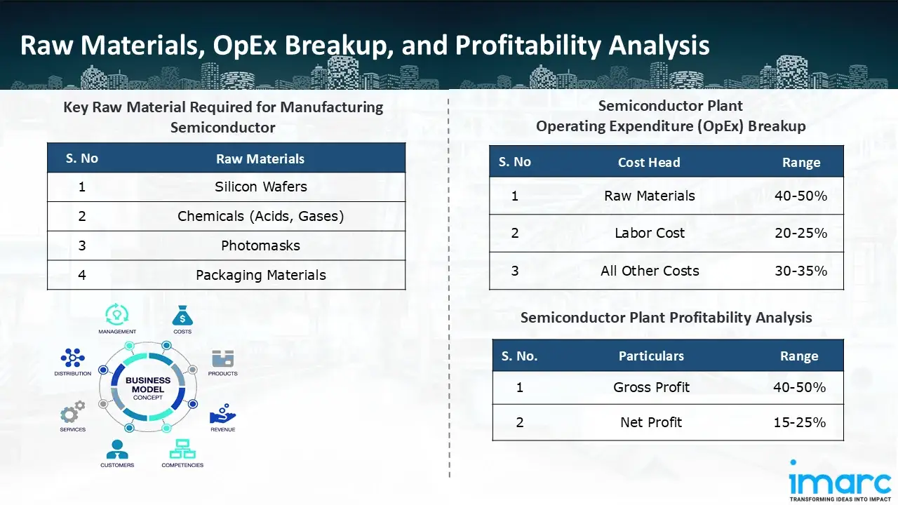
The basic raw materials required for semiconductor manufacturing include:
- Silicon Wafers
- Chemicals (Acids, Gases)
- Photomasks
- Packaging Materials
Machine Section or Lines Required:
- Wafer Fabrication (Lithography, Etching, Doping, Deposition)
- Testing
- Assembly
- Packaging
Techno-Commercial Parameter:
- Capital Expenditure (CapEx): Capital expenditure (CapEx) in a manufacturing plant includes various investments essential for its setup and long-term operations. It covers machinery and equipment costs, including procurement, installation, and commissioning. Civil works expenses involve land development, factory construction, and infrastructure setup. Utilities such as power, water supply, and HVAC systems are also significant. Additionally, material handling systems, automation, environmental compliance, and safety measures are key components. Other expenditures include IT infrastructure, security systems, and office essentials, ensuring operational efficiency and business growth.
- Operating Expenditure (OpEx): Operating expenditure is the cost incurred to operate a manufacturing plant effectively. OpEx in a manufacturing plant typically includes the cost of raw materials, utilities, depreciation, taxes, packing cost, transportation cost, and repairs and maintenance. The operating expenses are part of the cost structure of a manufacturing plant and have a significant effect on profitability and efficiency. Effective control of these costs is necessary for maintaining competitiveness and growth. Furthermore, raw material cost in semiconductor manufacturing plant ranges between 40-50%, labor cost ranges between 20% to 25%, and all other costs ranges between 30-35% in the proposed plant.
- Profitability Analysis Year on Year Basis: We assisted our client in developing a detailed cost model, which projects steady growth, with revenue rising throughout the projected period. Moreover, gross profit margins lie between a range of 40-50%, and net profit lie between the range of 15-25% during the income projection years, highlighting strong financial viability and profitability.
Conclusion & IMARC's Impact:
Our financial model for the semiconductor manufacturing plant was meticulously developed to meet the client’s objectives, providing an in-depth analysis of production costs, including raw materials, manufacturing, capital expenditure, and operational expenses. By addressing the specific requirements of manufacturing 240,000 wafers of semiconductor annually, we successfully identified key cost drivers and projected profitability, considering market trends, inflation, and potential fluctuations in raw material prices. This comprehensive financial model equipped the client with valuable insights into strategic decision-making, demonstrating our commitment to delivering high-quality, client-focused solutions that ensure the long-term success of large-scale manufacturing ventures.
Latest News and Developments:
- In December 2025, Taiwan Semiconductor Manufacturing Company (TSMC), has announced that it has begun mass producing its 2-nanometer (nm) devices, a significant advancement in semiconductor technology. Its most cutting-edge technology to date is represented by the new 2nm manufacturing node. The processors are made to perform better than the 3nm chipset.
- In November 2025, the installation of industrial gear at SK Hynix's new M15X fabrication plant in Cheongju, North Chungcheong Province, is a major step towards increasing the manufacturing of high bandwidth memory (HBM) in Korea.
- In October 2025, GlobalFoundries declared that it would invest €1.1 billion to increase its manufacturing capacity at its location in Dresden, Germany. By the end of 2028, the investment will enable a production capacity rise to over one million wafers annually, making it the largest plant of its kind in Europe.
Why Choose IMARC?
IMARC's Financial Model Expertise: Helping Our Clients Explore Industry Economics
IMARC is a global market research company that offers a wide range of services, including market entry and expansion, market entry and opportunity assessment, competitive intelligence and benchmarking, procurement research, pricing and cost research, regulatory approvals and licensing, factory setup, factory auditing, company incorporation, incubation services, recruitment services, and marketing and sales.
Under our factory setup services, we assist our clients in exploring the feasibility of their plants by providing comprehensive financial modeling. Additionally, we offer end-to-end consultation for setting up a plant in India or abroad. Our financial modeling includes an analysis of capital expenditure (CapEx) required to establish the manufacturing facility, covering costs such as land acquisition, building infrastructure, purchasing high-tech production equipment, and installation. Furthermore, the layout and design of the factory significantly influence operational efficiency, energy consumption, and labor productivity, all of which impact long-term operational expenditure (OpEx). So, every parameter is covered in the analysis.
At IMARC, we leverage our comprehensive market research expertise to support companies in every aspect of their business journey, from market entry and expansion to operational efficiency and innovation. By integrating our factory setup services with our deep knowledge of industry dynamics, we empower our clients to not only establish manufacturing facilities but also strategically position themselves in highly competitive markets. Our financial modeling and end-to-end consultation services ensure that clients can explore the feasibility of their plant setups while also gaining insights into competitors' strategies, technological advancements, and regulatory landscapes. This holistic approach enables our clients to make informed decisions, optimize their operations, and align with sustainable practices, ultimately driving long-term success and growth.
Our Clients


Contact Us
Have a question or need assistance?
Please complete the form with your inquiry or reach out to us at
Phone Number
+91-120-433-0800+1-201-971-6302
+44-753-714-6104
Previous Post

The retail landscape is experiencing a profound transformation as self-checkout systems emerge as critical infrastructure components reshaping consumer experiences and operational efficiency globally. These automated solutions enable customers to independently scan, bag, and pay for purchases without cashier assistance, representing a fundamental shift in modern commerce.
The webcams market is experiencing unprecedented transformation as digital communication becomes the cornerstone of modern business, education, and healthcare. Global webcam industry dynamics are being reshaped by technological innovation and evolving workplace models.
As smartphones become a way of life for most Filipinos, the market has changed dramatically and expectations from consumers are higher than ever before. With the demand for smartphones growing, there is a significant change in consumer shopping habits with more emphasis on using online platforms for shopping. This change is closely interlinked with the fast growth of the Philippines e-commerce market, both bringing opportunities and challenges to the stakeholders of the smartphone industry.
As technology continues to advance, lighting has transformed from a basic necessity into a strategic enabler of innovation, efficiency, and sustainability. The evolution from incandescent bulbs to LEDs, smart systems, and intelligent lighting networks represents not just technological change but a redefinition of how energy, design, and functionality intersect in the built environment.
An LED light is an illuminating device that utilizes Light Emitting Diodes as its source of light, generating light through a semiconductor-based process called electroluminescence. When electrical current flows across the semiconductor material of the diode, electrons emit energy as photons and thus produce highly efficient and concentrated illumination.
An LED bulb is a solid-state lighting device that uses Light Emitting Diodes (LEDs) as its illumination source. Different from incandescent or fluorescent lamps, light in LED bulbs is produced by electroluminescence, a process where the passing of an electric current through a semiconductor material emits photons directly. This process is highly energy-efficient, with a far larger percentage of the electricity being converted to usable light and very little heat generated in the process.
The junction box, generally made from plastic, metal, or composite materials, houses wire connections, terminations, and protective components to allow the safe distribution and routing of electrical circuits. The junction box will provide insulation, mechanical protection, and a secure environment to avoid accidental contact with live electrical parts, moisture intrusion, or dust accumulation.
The Japan power electronics market is poised to grow substantially, driven by rising demand in automotive, energy, industrial automation, and infrastructure sectors. According to IMARC Group, the Japan power electronics market is studied from 2019 to 2024 with projections extending to 2033.
Japan's printed circuit board (PCB) industry is the world leader in technology innovation, enabling consumer electronics, automotive, and next-generation communication system development. As a key enabler of modern electronic products, PCBs provide the essential building blocks for embedding semiconductors, sensors, and microchips into miniaturized, high-performance devices. Japan, through its world-class manufacturing base and engineering expertise, remains the hub of the global PCB supply chain.
Aluminum-Air (Al-Air) battery is a new energy storage technology that has attracted interest as a future alternative to conventional lithium-ion batteries, specifically for electric vehicle (EV) use. As opposed to normal rechargeable batteries, the Al-Air battery is a metal-air electrochemical cell with aluminum as the anode, oxygen from the ambient air as the cathode reactant, and a liquid electrolyte (commonly sodium hydroxide or potassium hydroxide) as the medium through which the reaction occurs.
Aluminium wire is an essential industrial commodity commonly employed in power transmission, electrical distribution, building construction, and manufacturing processes owing to its high conductivity-to-weight ratio, resistance to corrosion, and cost advantage over copper. Produced by methods including continuous casting, rolling, and drawing, aluminum wire is available in various grades and alloys to serve the wide demands, from overhead transmission conductors and building wiring to automotive harnesses and electronic applications.
Air conditioners are electromechanical devices used to control indoor climate by extracting heat and humidity and ensuring optimum air circulation. Generally consisting of a compressor, condenser, evaporator, refrigerant fluid, filters, fans, and electronic controls, air conditioners work based on the principle of heat exchange, moving heat from indoor areas to the external environment. Contemporary units come in diverse configurations, such as split systems, window units, central air systems, and portable models, supporting respective residential, commercial, and industrial applications. Some of the major characteristics are efficiency in cooling, energy use, noise rating, and environmental footprint in relation to refrigerant type.
E-waste, or electronic waste, is electrical and electronic equipment that has been discarded, such as computers, cell phones, television sets, servers, and household appliances. It is among the world's fastest-growing streams of waste, consisting of a heterogeneous combination of metals, plastics, glass, and toxic substances. E-waste contains valuable metals like copper, aluminum, gold, silver, palladium, and rare earth elements, in addition to toxic materials like lead, mercury, cadmium, and brominated flame retardants.
Polished silicon wafers are very pure, ultra-flat semiconductor substrates that are produced from high-quality single-crystal silicon. The wafers act as the material base for making integrated circuits, power devices, and MEMS (Microelectromechanical Systems). The wafers are made of monocrystalline silicon ingots using the Czochralski or Float-Zone process, from which the wafers are cut, lapped, etched, and polished to atomic-scale flatness and defect-free surfaces.
AI is revolutionizing Japan’s semiconductor industry by boosting innovation and efficiency across the entire value chain. Advanced artificial intelligence (AI)-powered Electronic Design Automation (EDA) tools significantly shorten chip design cycles, improving performance and energy efficiency.
Recent projections indicate that Australia semiconductor market, including services, is growing at a steady compound annual growth rate as the nation deepens its tech infrastructure. The importance of semiconductors spans electronics, defense systems, telecommunications, and emerging AI applications, which position the local ecosystem as strategically vital for growth.
Fiber optic cables are high-tech communications cables that carry information like bursts of light along extremely thin glass or plastic strands, providing high-speed, high-bandwidth connectivity with little loss of signal. Fiber optic cables make up the foundation of contemporary telecommunications, carrying internet, cloud computing, 5G networks, and smart infrastructure.
CAT (Category) cables are twisted-pair Ethernet cables utilized for copper-based wired network communications, varying from CAT5e to CAT8 standards. The cables carry data through copper conductors, but with different speeds (up to 40 Gbps for CAT8) and bandwidths, supporting networks such as LANs, data centers, and smart buildings.
India's semiconductor industry is undergoing a revolutionary phase driven by rising demand from industries like consumer electronics, automotive technologies, industrial automation, and telecom infrastructure.
USB data cables are critical elements of contemporary digital connectivity, enabling high-speed and consistent data transfer and power supply for a broad scope of electronic products. They provide the foundation for charging and synchronizing smartphones, tablets, laptops, and other peripherals, with significant applications in consumer electronics, industrial automation, and new technologies. With technologies like USB-C, the cables today carry faster data speeds, more power output, and universal compatibility, making them essential in a world that is connected.
Thin-film-transistor (TFT) liquid-crystal display (LCD) is a type of display technology used in many electronic devices, such as smartphones, tablets, laptops, and televisions (TVs). A backlight, colour filters, a thin-film transistor array, and a liquid crystal layer are among the layers that make up this flat-panel display. TFT LCDs are made to produce sharp images with superb viewing angles, strong contrast, and accurate colour reproduction. They are made up of thousands of tiny transistors that regulate how much light enters each pixel. This makes it possible for the display to generate crisp, detailed images at rapid refresh rates. TFT LCD technology's low power consumption is one of its main benefits, which makes it perfect for battery-operated gadgets.
Polycrystalline solar photovoltaic (PV) modules are a key component of solar energy systems, harnessing sunlight and converting it into electricity through the photovoltaic effect. These modules are composed of multiple interconnected solar cells, each made from polycrystalline silicon. Polycrystalline solar panels are renowned for their efficiency, affordability, and versatility, making them a popular choice for various applications such as solar installations, commercial and industrial projects, off-grid systems and solar farms.
The LED chip is the core component of an LED bulb, comprising semiconductor layers that enable the free flow of protons and electrons. Employed in all LED lighting fixtures—from bulbs to tubes—the LED chip fundamentally determines light quality, with variations in brightness, voltage, and wavelength. These chips are manufactured through a process called MOCVD (metal-organic chemical vapor deposition), which creates the semiconductor layers that facilitate electric flow. Major applications of these chips include backlighting, illumination, automotive lighting, signs, and signals.
Semiconductors are crucial components in the modern electronics industry, used in electronic equipment and devices to manage and control the flow of electricity. They are found in consumer items like smartphones, wearables, smart TVs, and advanced equipment used in industrial applications, defense, and aerospace. Semiconductors are further divided into four broad categories: optoelectronics, discrete components, integrated circuits, and sensors. Memory devices, logic devices, analog ICs, MPUs, discrete power devices, MCUs, and sensors are some of the major components of semiconductors.