Semiconductor Manufacturing Cost Analysis
Case Study: Cost Model for Semiconductor Manufacturing Plant
|
Client Request: Comprehensive financial feasibility study for a medium-scale semiconductor fab Location: India (Greenfield Setup) Plant Capacity: 240,000 silicon wafers per year Deliverable: Full DPR + 10-year financial model covering CapEx, OpEx, and profitability |
What is Semiconductor Manufacturing?
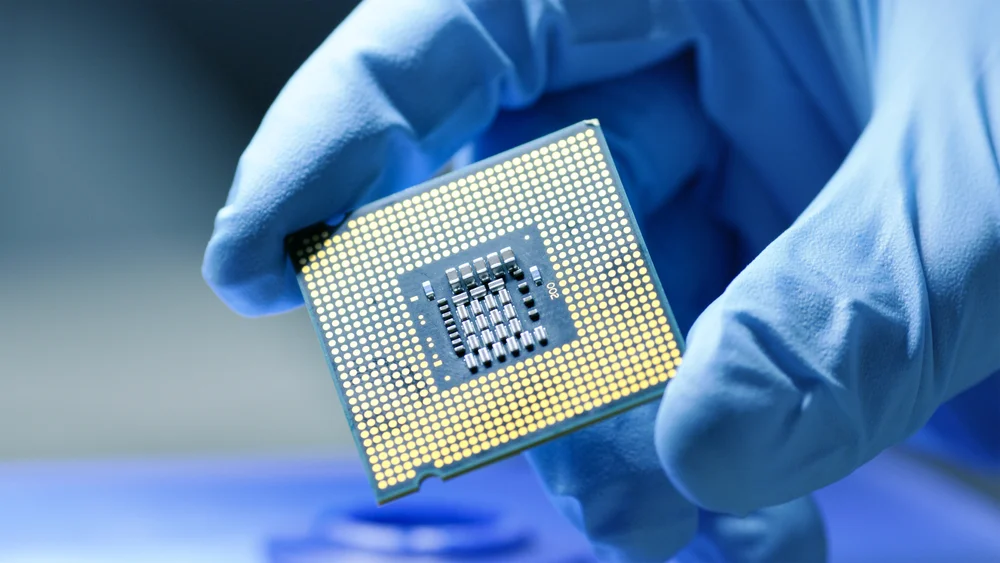
Semiconductor manufacturing transforms raw silicon into the electronic components that drive modern civilization — integrated circuits (ICs), memory chips, microprocessors, sensors, and discrete devices. The process requires extreme precision at the nanoscale, combining materials science, photolithography, and automated engineering under tightly controlled cleanroom conditions.
Core Process Summary
- Raw silicon is refined and grown into single-crystal ingots
- Ingots are sliced into ultra-thin wafers and polished to atomic flatness
- Circuits are patterned layer by layer via photolithography
- Devices are tested, diced, assembled into packages, and quality-certified
The result: every smartphone, data center, electric vehicle, medical device, and satellite depends on semiconductor components manufactured through this process.
Global Market Overview & Growth Drivers
|
Global Market (2024) $694 Billion |
Projected by 2033 $1.22 Trillion |
CAGR (2025–2033) 6.48% |
Plant Capacity 240,000 wafers/yr |
What Is Driving This Growth?
|
Growth Driver |
Explanation |
|
AI & Machine Learning |
Demands for high-performance logic chips, GPUs, and HBM memory are growing rapidly with AI infrastructure buildout. |
|
Automotive Electrification |
EVs and ADAS systems require 2–3x more semiconductors per vehicle versus traditional ICE vehicles. |
|
5G & Telecom Infrastructure |
Next-gen base stations, routers, and optical networks require advanced RF and processing chips. |
|
Industrial Automation (IIoT) |
Smart factories, robotics, and real-time sensors are expanding demand for durable, high-reliability chips. |
|
Government Policy & Subsidies |
The US CHIPS Act, India's PLI scheme, and EU Chips Act are funding new domestic fab capacity. |
|
Edge Computing & IoT |
Billions of connected devices require low-power, high-efficiency semiconductor components at the network edge. |
Key End-Use Applications
Semiconductors are foundational components across virtually every major industry. Below is a sector-by-sector breakdown of where demand originates:
|
Industry Sector |
Semiconductor Applications |
|
Consumer Electronics |
Smartphones, laptops, tablets, TVs, gaming consoles, wearables — processing, connectivity, and display. |
|
Data Centers & Cloud |
Server CPUs, GPUs, HBM memory, and networking chips powering cloud and AI workloads. |
|
Automotive & EV |
ECUs, ADAS, BMS, power inverters, infotainment — semiconductor content per vehicle is rising sharply. |
|
Industrial & Robotics |
PLCs, motion controllers, industrial sensors, IIoT gateways, real-time monitoring systems. |
|
Healthcare & Diagnostics |
Medical imaging, patient monitors, wearable health sensors, diagnostic instruments. |
|
Telecom & 5G |
5G base stations, routers, RF chips, and optical communication modules. |
|
Energy & Smart Grid |
Solar inverters, grid management systems, EV charging infrastructure, power electronics. |
|
Defense & Aerospace |
Navigation, radar, satellite communication, surveillance — high-reliability, rad-hard semiconductors. |
IMARC's Approach
IMARC Group developed a detailed techno-commercial financial model from the ground up. The model covered all phases of investment — from land acquisition and civil construction through equipment procurement, staffing, working capital, and year-on-year revenue and profit projections. Scenario analysis was included to account for raw material price fluctuations and inflation sensitivity.
Manufacturing Process: 8 Key Stages
Semiconductor manufacturing is a multi-stage, highly automated process requiring nanoscale precision at each step. Below is a stage-by-stage breakdown relevant to cost modeling:
|
Process Stage |
What Happens |
|
Stage 1: Silicon Ingot Production |
Ultra-pure silicon is melted and grown into single-crystal ingots using the Czochralski or float-zone method. This is the foundation of every wafer. |
|
Stage 2: Wafer Slicing & Polishing |
Ingots are precision-cut into thin wafers using diamond saws, then lapped, etched, and polished to atomic-level flatness inside a cleanroom. |
|
Stage 3: Photolithography |
A light-sensitive photoresist is applied and exposed to UV or EUV light through a photomask, transferring the nanoscale circuit pattern onto the wafer surface. |
|
Stage 4: Etching & Thin-Film Deposition |
Dry plasma or wet chemical etching removes unwanted material. CVD, PVD, or ALD techniques then deposit precise layers of conductive, insulating, or semiconductor films. |
|
Stage 5: Doping (Ion Implantation) |
Controlled impurities are introduced via ion implantation or diffusion to precisely modify the silicon's electrical characteristics and enable transistor formation. |
|
Stage 6: Metrology & Process Control |
Advanced metrology tools monitor critical dimensions, alignment, and film uniformity at the nanometer scale — the quality gate between every major process step. |
|
Stage 7: Assembly & Packaging |
Functional dies are diced from the wafer, mounted onto substrates, connected via wire bonding or flip-chip, and encapsulated in protective packages. |
|
Stage 8: Testing & Quality Assurance |
Final burn-in testing, electrical validation, and comprehensive QA checks ensure every device meets performance, reliability, and customer-specified standards before shipment. |
Each of the stages above involves specific capital equipment, consumables, utilities, and skilled labor — all of which are captured in the CapEx and OpEx models developed for this client.
Plant Inputs: Raw Materials & Equipment
Key Raw Materials
|
Raw Material |
Role in Process |
|
Silicon Wafers |
Primary substrate — 200mm or 300mm polished wafers |
|
Process Chemicals |
HF, H2SO4, H2O2, NH4OH — used in cleaning and wet etching |
|
Specialty Gases |
Silane, nitrogen, argon, chlorine — for CVD, etching, and doping |
|
Photomasks |
Quartz masks with circuit patterns for each lithography layer |
|
Photoresist |
Light-sensitive polymer applied before each patterning step |
|
CMP Slurries |
Abrasive suspensions for chemical-mechanical planarization |
|
Dielectric Films |
Oxide and nitride layers for insulation and passivation |
|
Packaging Materials |
Lead frames, substrates, bonding wire, molding compound, solder |
Key Equipment & Machinery Lines
|
Equipment Line |
Function |
|
Photolithography Systems |
EUV or DUV scanners for pattern transfer — highest CapEx item |
|
Etch Systems |
Plasma etch chambers for dry etching of patterns |
|
CVD / PVD / ALD Tools |
Thin-film deposition equipment for insulating and conductive layers |
|
Ion Implanters |
Introduces dopants at controlled energy and dose into the wafer |
|
CMP Systems |
Polishing tools to flatten each deposited layer |
|
Wafer Inspection Tools |
Optical and e-beam metrology for defect detection and CD measurement |
|
Dicing Saws / Laser Dicers |
Singulate individual dies from the fabricated wafer |
|
Wire Bonders / Flip-Chip |
Interconnect packaging equipment for electrical connections |
Cost Model: Capital Expenditure (CapEx)
Capital expenditure covers all one-time investments required to establish the semiconductor manufacturing facility. For a 240,000 wafer/year plant in India, CapEx is distributed across the following heads:
|
CapEx Component |
Approx. Share |
|
Machinery & Equipment (procurement, installation, commissioning) |
~45% of total CapEx |
|
Civil Works: land development, factory construction, cleanroom build |
~20% of total CapEx |
|
Cleanroom Infrastructure: HVAC, air handling, vibration isolation |
~15% of total CapEx |
|
Utilities: power supply, UPS, water treatment, effluent systems |
~8% of total CapEx |
|
Material Handling & Automation Systems |
~7% of total CapEx |
|
IT Infrastructure, ERP, safety & compliance systems |
~5% of total CapEx |
Note: Cleanroom construction and lithography equipment alone typically constitute 50–60% of the total CapEx for a semiconductor fab. Equipment lead times of 12–24 months must be factored into project scheduling.
Cost Model: Operating Expenditure (OpEx)
Operating expenditure covers all recurring costs to run the plant at designed capacity. For a 240,000 wafer/year semiconductor facility, the cost structure is as follows:
|
OpEx Component |
Approx. Share |
|
Raw Materials (silicon wafers, chemicals, gases, photomasks) |
40–50% of total OpEx |
|
Skilled Labor & Workforce (engineers, technicians, operators) |
20–25% of total OpEx |
|
Utilities: power, DI water, chilled water, cleanroom HVAC |
~8% of total OpEx |
|
Repairs, Maintenance & Spare Parts |
~6% of total OpEx |
|
Depreciation & Amortization on Equipment |
~5% of total OpEx |
|
Quality Control, Testing & Certification |
~3% of total OpEx |
|
Packaging, Logistics & Outbound Freight |
~3% of total OpEx |
|
Overheads: administration, insurance, compliance |
~3–5% of total OpEx |
|
Key Cost Driver Insight: Raw materials account for the largest share of operating costs (40–50%). Silicon wafer prices and specialty chemical costs are the primary variables that affect gross margin sensitivity. A 10% increase in raw material costs typically compresses gross margins by 4–5 percentage points. |
Profitability Analysis: Year-on-Year Financial Projections
IMARC's financial model projects a steady revenue ramp as the plant moves from initial production to full capacity. The model accounts for ramp-up losses in Years 1–2, yield improvement curves, inflation, and raw material price sensitivity.
|
Financial Metric |
Range / Outcome |
Notes |
|
Gross Profit Margin |
40% – 50% |
Sustained across projection period with volume scale |
|
Net Profit Margin |
15% – 25% |
After depreciation, interest, and income tax obligations |
|
Revenue Trend |
↑ Steady Growth |
Rising throughout the 10-year projection horizon |
|
Breakeven Timeline |
Year 3–4 |
Typical for a medium-scale semiconductor fab in India |
|
IRR (Indicative) |
18% – 25% |
Depends on wafer yield, ASP, and subsidy utilization |
|
Payback Period |
6–8 Years |
Consistent with capital-intensive semiconductor industry norms |
These margins demonstrate strong financial viability. India's Production Linked Incentive (PLI) scheme for semiconductors provides additional upside through capital subsidies (up to 50% of project cost) and design-linked incentives, improving effective IRR by 3–5 percentage points.
Latest Industry Developments
|
Development |
Details |
|
December 2025 — TSMC |
Began mass production of 2-nanometer devices — the company's most advanced node yet, delivering superior performance over the previous 3nm generation. |
|
November 2025 — SK Hynix |
Completed industrial equipment installation at M15X fab in Cheongju, South Korea, significantly expanding high bandwidth memory (HBM) production capacity. |
|
October 2025 — GlobalFoundries |
Committed €1.1 billion to expand its Dresden, Germany site. By end of 2028, capacity will exceed 1 million wafers/year — the largest such facility in Europe. |
Conclusion: IMARC's Impact
IMARC Group delivered a rigorous, data-driven financial model that equipped the client with a full picture of their investment — from first rupee of capital to projected Year 10 profitability. The model identified the key cost drivers, stress-tested assumptions across scenarios, and provided a clear basis for board-level investment decisions and bank financing.
What the Model Covered
- Full CapEx schedule with phased equipment procurement and civil works timeline
- Operating cost model with sensitivity to raw material prices and yield rates
- Year-on-year revenue projections based on wafer ASP benchmarks and capacity ramp
- Gross margin, EBITDA, and net profit projections across a 10-year horizon
- IRR, NPV, and payback period analysis for investor and lender presentation
- PLI scheme subsidy impact analysis and effective cost-of-project recalculation
Why Choose IMARC Group?
IMARC Group is a global market research and consulting firm with specialized expertise in techno-commercial feasibility studies, DPR reports, and plant setup advisory across 50+ industries. Our semiconductor cost models are built on real equipment pricing, current market data, and region-specific labor and utility benchmarks — not templates.
Our Services for Investors & Project Developers
- Detailed Project Report (DPR) for semiconductor and electronics manufacturing plants
- CapEx and OpEx modeling for greenfield and brownfield fab setups
- Market feasibility studies for new product lines or geographies
- Competitive intelligence and benchmarking against global fab operators
- Site selection analysis: land, utilities, labor, and incentive comparison across states
- Regulatory compliance mapping: environmental clearances, BIS, CPCB approvals
- End-to-end plant setup consulting: from site acquisition to production ramp-up
Our Clients


Contact Us
Have a question or need assistance?
Please complete the form with your inquiry or reach out to us at
Phone Number
+91-120-433-0800+1-201-971-6302
+44-753-714-6104
Previous Post

The hearables market represents one of the most dynamic segments within consumer electronics and wearable technology. These intelligent audio devices have evolved beyond simple wireless earbuds into multifunctional platforms combining premium audio with health monitoring, artificial intelligence, and seamless digital connectivity.
A smart washing machine is a sophisticated home appliance that incorporates advanced digital features such as connectivity, sensor technology, and automated controls for improved efficiency, convenience, and user control. In contrast to traditional washing machines, smart washing machines come pre-installed with advanced features such as Wi-Fi connectivity, smart load detection, smart detergent dispensing, and voice-control capability.
A smartphone is a portable electronic device that combines sophisticated capabilities in computer processing, wireless communication, multimedia entertainment, and internet access. Smartphones are distinct from other mobile phones in that their operation involves highly sophisticated platforms of operation that are capable of supporting multiple applications, multitasking, and connectivity with internet platforms.
Semiconductor manufacturing is a highly specialized industrial process that involves the design, fabrication, and assembly of semiconductor devices including integrated circuits (ICs), memory chips, sensors, and discrete components. The process transforms raw semiconductor materials, primarily silicon, into sophisticated electronic components through a combination of physical and chemical processing steps, such as wafer fabrication, photolithography, doping, etching, thin-film deposition, and packaging.
The retail landscape is experiencing a profound transformation as self-checkout systems emerge as critical infrastructure components reshaping consumer experiences and operational efficiency globally. These automated solutions enable customers to independently scan, bag, and pay for purchases without cashier assistance, representing a fundamental shift in modern commerce.
The webcams market is experiencing unprecedented transformation as digital communication becomes the cornerstone of modern business, education, and healthcare. Global webcam industry dynamics are being reshaped by technological innovation and evolving workplace models.
As smartphones become a way of life for most Filipinos, the market has changed dramatically and expectations from consumers are higher than ever before. With the demand for smartphones growing, there is a significant change in consumer shopping habits with more emphasis on using online platforms for shopping. This change is closely interlinked with the fast growth of the Philippines e-commerce market, both bringing opportunities and challenges to the stakeholders of the smartphone industry.
As technology continues to advance, lighting has transformed from a basic necessity into a strategic enabler of innovation, efficiency, and sustainability. The evolution from incandescent bulbs to LEDs, smart systems, and intelligent lighting networks represents not just technological change but a redefinition of how energy, design, and functionality intersect in the built environment.
An LED light is an illuminating device that utilizes Light Emitting Diodes as its source of light, generating light through a semiconductor-based process called electroluminescence. When electrical current flows across the semiconductor material of the diode, electrons emit energy as photons and thus produce highly efficient and concentrated illumination.
An LED bulb is a solid-state lighting device that uses Light Emitting Diodes (LEDs) as its illumination source. Different from incandescent or fluorescent lamps, light in LED bulbs is produced by electroluminescence, a process where the passing of an electric current through a semiconductor material emits photons directly. This process is highly energy-efficient, with a far larger percentage of the electricity being converted to usable light and very little heat generated in the process.
The junction box, generally made from plastic, metal, or composite materials, houses wire connections, terminations, and protective components to allow the safe distribution and routing of electrical circuits. The junction box will provide insulation, mechanical protection, and a secure environment to avoid accidental contact with live electrical parts, moisture intrusion, or dust accumulation.
The Japan power electronics market is poised to grow substantially, driven by rising demand in automotive, energy, industrial automation, and infrastructure sectors. According to IMARC Group, the Japan power electronics market is studied from 2019 to 2024 with projections extending to 2033.
Japan's printed circuit board (PCB) industry is the world leader in technology innovation, enabling consumer electronics, automotive, and next-generation communication system development. As a key enabler of modern electronic products, PCBs provide the essential building blocks for embedding semiconductors, sensors, and microchips into miniaturized, high-performance devices. Japan, through its world-class manufacturing base and engineering expertise, remains the hub of the global PCB supply chain.
Aluminum-Air (Al-Air) battery is a new energy storage technology that has attracted interest as a future alternative to conventional lithium-ion batteries, specifically for electric vehicle (EV) use. As opposed to normal rechargeable batteries, the Al-Air battery is a metal-air electrochemical cell with aluminum as the anode, oxygen from the ambient air as the cathode reactant, and a liquid electrolyte (commonly sodium hydroxide or potassium hydroxide) as the medium through which the reaction occurs.
Aluminium wire is an essential industrial commodity commonly employed in power transmission, electrical distribution, building construction, and manufacturing processes owing to its high conductivity-to-weight ratio, resistance to corrosion, and cost advantage over copper. Produced by methods including continuous casting, rolling, and drawing, aluminum wire is available in various grades and alloys to serve the wide demands, from overhead transmission conductors and building wiring to automotive harnesses and electronic applications.
Air conditioners are electromechanical devices used to control indoor climate by extracting heat and humidity and ensuring optimum air circulation. Generally consisting of a compressor, condenser, evaporator, refrigerant fluid, filters, fans, and electronic controls, air conditioners work based on the principle of heat exchange, moving heat from indoor areas to the external environment. Contemporary units come in diverse configurations, such as split systems, window units, central air systems, and portable models, supporting respective residential, commercial, and industrial applications. Some of the major characteristics are efficiency in cooling, energy use, noise rating, and environmental footprint in relation to refrigerant type.
E-waste, or electronic waste, is electrical and electronic equipment that has been discarded, such as computers, cell phones, television sets, servers, and household appliances. It is among the world's fastest-growing streams of waste, consisting of a heterogeneous combination of metals, plastics, glass, and toxic substances. E-waste contains valuable metals like copper, aluminum, gold, silver, palladium, and rare earth elements, in addition to toxic materials like lead, mercury, cadmium, and brominated flame retardants.
Polished silicon wafers are very pure, ultra-flat semiconductor substrates that are produced from high-quality single-crystal silicon. The wafers act as the material base for making integrated circuits, power devices, and MEMS (Microelectromechanical Systems). The wafers are made of monocrystalline silicon ingots using the Czochralski or Float-Zone process, from which the wafers are cut, lapped, etched, and polished to atomic-scale flatness and defect-free surfaces.
AI is revolutionizing Japan’s semiconductor industry by boosting innovation and efficiency across the entire value chain. Advanced artificial intelligence (AI)-powered Electronic Design Automation (EDA) tools significantly shorten chip design cycles, improving performance and energy efficiency.
Recent projections indicate that Australia semiconductor market, including services, is growing at a steady compound annual growth rate as the nation deepens its tech infrastructure. The importance of semiconductors spans electronics, defense systems, telecommunications, and emerging AI applications, which position the local ecosystem as strategically vital for growth.
Fiber optic cables are high-tech communications cables that carry information like bursts of light along extremely thin glass or plastic strands, providing high-speed, high-bandwidth connectivity with little loss of signal. Fiber optic cables make up the foundation of contemporary telecommunications, carrying internet, cloud computing, 5G networks, and smart infrastructure.
CAT (Category) cables are twisted-pair Ethernet cables utilized for copper-based wired network communications, varying from CAT5e to CAT8 standards. The cables carry data through copper conductors, but with different speeds (up to 40 Gbps for CAT8) and bandwidths, supporting networks such as LANs, data centers, and smart buildings.
India's semiconductor industry is undergoing a revolutionary phase driven by rising demand from industries like consumer electronics, automotive technologies, industrial automation, and telecom infrastructure.
USB data cables are critical elements of contemporary digital connectivity, enabling high-speed and consistent data transfer and power supply for a broad scope of electronic products. They provide the foundation for charging and synchronizing smartphones, tablets, laptops, and other peripherals, with significant applications in consumer electronics, industrial automation, and new technologies. With technologies like USB-C, the cables today carry faster data speeds, more power output, and universal compatibility, making them essential in a world that is connected.
Thin-film-transistor (TFT) liquid-crystal display (LCD) is a type of display technology used in many electronic devices, such as smartphones, tablets, laptops, and televisions (TVs). A backlight, colour filters, a thin-film transistor array, and a liquid crystal layer are among the layers that make up this flat-panel display. TFT LCDs are made to produce sharp images with superb viewing angles, strong contrast, and accurate colour reproduction. They are made up of thousands of tiny transistors that regulate how much light enters each pixel. This makes it possible for the display to generate crisp, detailed images at rapid refresh rates. TFT LCD technology's low power consumption is one of its main benefits, which makes it perfect for battery-operated gadgets.
Polycrystalline solar photovoltaic (PV) modules are a key component of solar energy systems, harnessing sunlight and converting it into electricity through the photovoltaic effect. These modules are composed of multiple interconnected solar cells, each made from polycrystalline silicon. Polycrystalline solar panels are renowned for their efficiency, affordability, and versatility, making them a popular choice for various applications such as solar installations, commercial and industrial projects, off-grid systems and solar farms.
The LED chip is the core component of an LED bulb, comprising semiconductor layers that enable the free flow of protons and electrons. Employed in all LED lighting fixtures—from bulbs to tubes—the LED chip fundamentally determines light quality, with variations in brightness, voltage, and wavelength. These chips are manufactured through a process called MOCVD (metal-organic chemical vapor deposition), which creates the semiconductor layers that facilitate electric flow. Major applications of these chips include backlighting, illumination, automotive lighting, signs, and signals.
Semiconductors are crucial components in the modern electronics industry, used in electronic equipment and devices to manage and control the flow of electricity. They are found in consumer items like smartphones, wearables, smart TVs, and advanced equipment used in industrial applications, defense, and aerospace. Semiconductors are further divided into four broad categories: optoelectronics, discrete components, integrated circuits, and sensors. Memory devices, logic devices, analog ICs, MPUs, discrete power devices, MCUs, and sensors are some of the major components of semiconductors.