Semiconductor Fabrication Manufacturing Plant Setup in India: Cost, Process Flow, Machinery, DPR & Financial Guide 2026
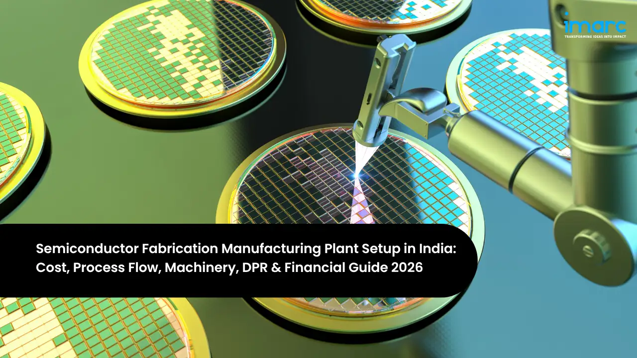
Setting up a Semiconductor Fabrication Manufacturing Plant in India is a highly capital-intensive but strategically transformative venture, driven by the country's semiconductor mission, deep policy incentives, and a vast import-substitution opportunity. Semiconductors are the foundation of every modern electronic and digital product, yet India currently imports almost all of its chip requirement. As the government backs domestic fabrication with large incentives and the global industry diversifies its supply chains, semiconductor fabrication has become one of the most significant industrial opportunities in the country's history.
Semiconductor Fabrication Manufacturing Plant cost in India depends enormously on technology node, wafer size, and whether the facility is a full wafer fab, a compound-semiconductor fab, or an assembly and test unit, with total investment ranging from a few hundred crore for a specialized or ATMP facility to tens of thousands of crore for a leading-edge wafer fab. Government incentives under the India Semiconductor Mission can cover a substantial share of project cost, materially improving project economics. Because of the scale and long build-out, payback periods are longer than in conventional manufacturing, typically 7 to 12 years, with returns underpinned by strategic demand and policy support.
This guide is designed for investors, entrepreneurs, and manufacturers evaluating entry into the Semiconductor Fabrication Market in India. It covers what the business involves, why demand is rising, the full fabrication process, machinery and materials, location and infrastructure planning, a detailed cost and financial breakdown, the licenses and approvals you must secure, and how a Detailed Project Report turns all of this into a bankable plan.
India Market Snapshot
| Key Facts | Details |
|---|---|
| India Semiconductor Market (2025) | USD 59.78 Billion (indicative, rising) |
| Import Dependence | Very high, almost all chips imported |
| Projected Market CAGR (2026–2032) | 15–20% (indicative) |
| Facility Types | Wafer fab, compound-semi fab, ATMP/OSAT |
| Indicative Total Investment | INR 500 – 50,000+ Crore |
| Typical Payback Period | 7–12 Years |
The snapshot captures why this sector is treated as nationally strategic: a very large and fast-growing market that is almost entirely served by imports, backed by exceptional policy support aimed at building a domestic semiconductor ecosystem. The enormous investment range reflects a fundamental choice of facility type, from an assembly and test unit or compound-semiconductor fab at the lower end to a leading-edge silicon wafer fab at the top. The rest of this guide unpacks that decision in detail.
Investment Highlights
Indicative Project Cost in India (2026)
| Parameter | Value |
|---|---|
| Facility Type | Wafer fab, compound-semi, or ATMP/OSAT |
| Total Project Investment | INR 500 – 50,000+ Crore |
| Payback Period | 7 – 12 Years |
| Government Incentive Support | Significant, via India Semiconductor Mission |
| Best Locations | Gujarat, Assam, Karnataka, Uttar Pradesh, Tamil Nadu |
| Mandatory Approvals | Factory Licence, CPCB/SPCB, Hazardous Waste, Fire NOC |
| Primary End Markets | Electronics, Automotive, Telecom, Computing |
| Key Enabler | Policy incentives and ecosystem partners |
These indicative parameters give a realistic frame for early feasibility work at a strategic level. The economics of semiconductor fabrication are unusual: capital costs are very high and payback is long, but government incentives, anchor customers, and technology partnerships can transform the picture. A well-prepared project report is essential here, because the scale, technology choice, and incentive structure must be modelled carefully before any commitment is made.
Table of Contents
- What is Semiconductor Fabrication?
- Why is Semiconductor Fabrication Growing in India?
- Semiconductor Fabrication Process
- Raw Materials and India Sourcing
- Location, Land & Infrastructure
- Machinery and Equipment Required
- Semiconductor Fabrication Manufacturing Plant Setup Cost in India (CapEx & OpEx)
- Financial Analysis and Profitability
- Licenses & Regulatory Approvals Required to setup Semiconductor Fabrication Manufacturing Plant in India
- Recent Developments in the India Semiconductor Fabrication Market
- How a Semiconductor Fabrication Manufacturing Plant Project Report (DPR) Helps Investors
- Frequently Asked Questions
What is Semiconductor Fabrication?
Semiconductor Fabrication is the process of building integrated circuits, or chips, on wafers of semiconductor material such as silicon. A Semiconductor Fabrication Manufacturing Plant, commonly called a fab, uses hundreds of precise photolithography, deposition, etching, and doping steps to create microscopic transistors and interconnections that form working circuits. The finished wafers are then cut, assembled, and tested into the chips that power every computing, communication, automotive, and consumer electronic device.
From a business perspective, what makes Semiconductor Fabrication strategically attractive in India is the combination of enormous, diversified demand and near-total current reliance on imports. A fabrication ecosystem that can meet quality and volume expectations addresses both a large commercial market and a national priority to secure the semiconductor supply chain.
- Computing & Data Centres: Processors, memory, and logic chips for computers, servers, and cloud infrastructure, a large and growing demand base.
- Consumer Electronics & Mobile: Chips for smartphones, appliances, and wearables, the highest-volume end market in India.
- Automotive & Power: Power and control chips for electric vehicles and industrial systems, a fast-growing high-reliability segment.
- Telecom & Defence: Communication and strategic chips where trusted, secure domestic supply is increasingly valued.
The Main Types of Semiconductor Facilities
Understanding which facility type you intend to build is the foundational decision, because scale, technology, and capital differ by orders of magnitude:
| Facility Type | Capital Scale | Key Property | Primary Role |
|---|---|---|---|
| Leading-Edge Wafer Fab | Very high | Advanced logic and memory nodes | High-volume chip fabrication |
| Mature-Node Fab | High | Established, cost-effective nodes | Automotive, industrial, power chips |
| Compound-Semiconductor Fab | Medium-high | Materials such as GaN and SiC | Power, RF, and EV applications |
| ATMP / OSAT | Medium | Assembly, test, and packaging | Back-end chip finishing |
This choice is the single most important early decision in the business, because it dictates the scale of capital, the technology partners you need, and the customers you can serve. Assembly, test, and packaging or compound-semiconductor facilities require far less capital and are a practical entry point into the ecosystem, while leading-edge wafer fabs demand extraordinary investment, deep technology partnerships, and long horizons. Many national semiconductor strategies begin by building assembly, test, and mature-node capability before moving toward advanced fabrication.
Why is Semiconductor Fabrication Growing in India?
Key Growth Drivers in the Indian Market
India's Semiconductor Fabrication market is being propelled by several structural factors that combine exceptional policy support with deep, diversified demand. Few industries enjoy this degree of deliberate national backing alongside a large addressable market:
- India Semiconductor Mission: Dedicated national policy and incentive programmes support the establishment of fabs, compound-semiconductor units, and assembly and test facilities, sharing a significant portion of project cost.
- Massive import substitution: India imports almost all of its semiconductor requirement, so domestic fabrication addresses one of the largest single import categories and a strategic vulnerability.
- Electronics manufacturing scale-up: Rapid growth in domestic electronics assembly, led by mobile phones and devices, is creating strong pull for locally made chips and components.
- Global supply-chain diversification: Global chip makers and their customers are diversifying manufacturing beyond a few concentrated locations, and India is positioning itself as a key alternative base.
- Automotive and digital demand: Electric mobility, digitization, and connectivity are expanding chip demand across automotive, industrial, and telecom sectors.
India-Specific Market Opportunity
| Sector | India Market Context | Semiconductor Role |
|---|---|---|
| Consumer Electronics | Booming mobile and device assembly | Largest-volume chip demand |
| Computing & Data | Growing IT and data-centre base | Logic and memory chips |
| Automotive & EV | Fast-growing electric mobility | Power and control chips |
| Telecom & Networking | Ongoing network expansion | Communication chips |
| Defence & Strategic | Localization and secure sourcing | Trusted domestic supply |
The strongest near-term opportunity for most investors lies in the back-end and specialized segments, such as assembly, test, and packaging or compound-semiconductor fabrication, which require far less capital than a leading-edge fab while still capturing a critical position in the ecosystem. These facilities serve domestic electronics assemblers who currently import finished chips and value a reliable, policy-supported local supplier. High-reliability sectors such as automotive and defence are especially attractive because they prize trusted domestic supply.
Semiconductor Fabrication Process
Understanding the fabrication process helps you plan equipment, ultra-clean infrastructure, and the main cost drivers. Semiconductor fabrication is among the most complex manufacturing processes in the world, involving hundreds of tightly controlled steps performed in an ultra-clean environment. The core flow, in simplified form, moves a wafer through repeated cycles of the following stages:
Process: Wafer Fabrication Route
In wafer fabrication, circuits are built up layer by layer on a silicon wafer through repeated patterning and processing. The sequence below is repeated many times to form the multiple layers of a modern chip, with each cycle adding transistors and interconnections under extremely precise control.
| Unit Operation | Key Activity |
|---|---|
| Wafer Preparation | Silicon wafers cleaned and prepared as the base substrate |
| Oxidation / Deposition | Thin insulating or conductive films grown or deposited |
| Photolithography | Circuit patterns transferred to the wafer using light and photoresist |
| Etching | Exposed material selectively removed to form features |
| Ion Implantation / Doping | Dopants introduced to create transistor regions |
| Deposition (CVD/PVD) | Additional material layers deposited |
| Chemical Mechanical Planarization | Wafer surface polished flat between layers |
| Metallization | Metal interconnects formed to wire the circuit |
| Wafer Test | Electrical testing of circuits on the wafer |
| Assembly, Test & Packaging | Wafers diced, packaged, and final-tested into chips |
Two points dominate the economics of this flow. First, yield is everything, because a single defect can ruin a chip, and even microscopic contamination lowers the proportion of working devices, so cleanliness and process control directly determine profitability. Second, the process depends on ultra-pure materials, specialized gases and chemicals, and extraordinarily precise equipment, which is why fabs require both deep technology partnerships and a highly skilled workforce to operate successfully.
Raw Materials and India Sourcing
Semiconductor fabrication depends on ultra-pure materials and specialized consumables, and while some are available domestically, many high-purity inputs are currently imported. Material purity and supply security are critical, because contamination or interruption directly affects yield and output, making sourcing strategy a central part of project planning.
| Material | Role in Process | India Sourcing | % of OpEx |
|---|---|---|---|
| Silicon Wafers | Base substrate for chips | Largely imported; localization emerging | 20–30% |
| Photoresists & Chemicals | Patterning and processing | Specialty suppliers, mostly imported | 10–18% |
| Specialty Gases | Deposition, etching, doping | Industrial gas suppliers | 8–15% |
| Ultra-Pure Water & Consumables | Rinsing and processing | On-site generation with local inputs | 5–10% |
| Packaging Materials | Assembly and packaging | Domestic and imported suppliers | 6–12% |
Because so many inputs are ultra-pure and currently imported, building reliable supplier relationships and, over time, encouraging domestic materials capacity is a strategic priority for the whole ecosystem. A fab must secure consistent, high-purity supply to protect yield, so sourcing agreements and buffer arrangements are essential. As India's semiconductor ecosystem develops under policy support, more of this materials supply chain is expected to localize, gradually improving cost and resilience for domestic fabricators.
Location, Land & Infrastructure
Where you set up your Semiconductor Fabrication Manufacturing Plant in India is a decision of strategic importance, because fabs require exceptional infrastructure: vast quantities of ultra-pure water, uninterrupted high-quality power, vibration-free construction, and a skilled talent base. State incentives and dedicated semiconductor zones also materially affect project viability.
Best States for Semiconductor Fabrication Plant Setup in India
| State | Why It Works | Key Advantage |
|---|---|---|
| Gujarat | Dedicated semiconductor policy and land | Strong state incentives and infrastructure |
| Assam | Emerging assembly and test hub | Policy-backed ecosystem investment |
| Karnataka | Deep electronics and design base | Skilled talent and design linkages |
| Uttar Pradesh | Large electronics manufacturing zones | Northern market and infrastructure |
| Tamil Nadu | Established electronics ecosystem | Manufacturing base and ports |
| Telangana | Growing electronics and IT hub | Talent and state support |
The strongest locations combine dedicated state semiconductor policy, reliable ultra-pure water and power, and access to skilled talent and design ecosystems. Gujarat has moved early with dedicated policy and land, while Karnataka and Tamil Nadu offer deep electronics and design talent, and Assam is emerging as an assembly and test hub under policy support. Because fabs are extraordinarily resource-intensive, water security, power quality, and state incentive alignment should weigh most heavily in the final choice.
Site Selection Criteria
- Ultra-pure water availability: Fabs consume very large volumes of ultra-pure water, so a secure, high-quality water source and treatment capability are essential and often decisive.
- Uninterrupted quality power: Even brief power fluctuations can ruin production, so stable, high-quality power with robust backup is a fundamental requirement.
- State incentives and zones: Dedicated semiconductor policies and industrial zones can share significant project cost and speed approvals, materially improving viability.
- Skilled talent access: Proximity to engineering talent and design ecosystems supports the highly skilled operations a fab requires.
- Vibration-free, clean environment: Sensitive equipment needs stable, low-vibration foundations and an ultra-clean setting, which shapes site and building design.
Infrastructure Requirements (Fab-Scale Facility)
| Infrastructure Element | Specification | India-Specific Note |
|---|---|---|
| Cleanroom | High-class controlled environment | Core of the fab; extremely demanding to build |
| Ultra-Pure Water System | Large-scale UPW plant | High and continuous water requirement |
| Power Requirement | Very high, uninterrupted | Quality and continuity are critical |
| Specialty Gas & Chemical Systems | Controlled supply and abatement | Safe handling of hazardous materials |
| Effluent & Emissions Treatment | Advanced treatment | Required under pollution-control norms |
| Vibration-Controlled Foundation | Stable, isolated base | Protects sensitive equipment |
| Skilled Workforce Facilities | Training and clean protocols | Supports complex operations |
Infrastructure for a semiconductor fab is in a different league from conventional manufacturing, because the cleanroom, ultra-pure water, and uninterrupted power systems are core to whether chips can be made at all. These systems represent a large share of both capital and operating cost, and under-provisioning any of them undermines yield and compliance. This is why fab projects are typically planned with technology partners and specialized engineering firms from the earliest stage.
Machinery and Equipment Required
Machinery is by far the largest capital expenditure in a Semiconductor Fabrication Manufacturing Plant, often well over half of total cost, and the equipment is among the most sophisticated and expensive in any industry. Because fabrication demands extreme precision and cleanliness, tools are highly specialized, largely imported, and supported by close vendor and technology partnerships. The line-up grows dramatically in cost and complexity with the technology node.
| Equipment | Function | Key Specification |
|---|---|---|
| Photolithography System | Pattern circuits on wafers | High-precision exposure tools |
| Etching Equipment | Remove material to form features | Dry and wet etch systems |
| Deposition Systems (CVD/PVD) | Deposit thin films | Precise, contamination-controlled |
| Ion Implanter | Dope transistor regions | Controlled dose and energy |
| CMP Equipment | Planarize wafer surfaces | Ultra-flat polishing |
| Diffusion / Oxidation Furnaces | Grow and treat films | Tightly controlled thermal process |
| Metrology & Inspection | Measure and inspect at nanoscale | Advanced defect detection |
| Wafer Test & Probe | Test circuits on wafers | High-accuracy electrical test |
| Assembly & Packaging Line | Dice, package, and test chips | Back-end finishing equipment |
| Facility & Abatement Systems | Support cleanroom and safety | Gas, chemical, and exhaust control |
Equipment selection follows directly from the facility type and technology node, and it is inseparable from the choice of technology partner, since advanced tools are supplied and supported by a small number of specialized global vendors. For an assembly, test, and packaging or compound-semiconductor facility, the equipment set is more accessible and less costly, which is why these routes are common entry points. Metrology and inspection capability is critical throughout, because detecting defects early protects yield in a process where each wafer carries enormous value.
Semiconductor Fabrication Manufacturing Plant Setup Cost in India (CapEx & OpEx)
The tables below give you a breakdown of both the upfront capital investment and the ongoing operating costs at a structural level, recognizing that absolute figures vary enormously by facility type. The actual cost for your specific plant will depend on the technology node, wafer size, facility type, and the level of incentive support secured.
Capital Expenditure (CapEx) Cost Structure
| CapEx Component | % of Total CapEx | What It Covers |
|---|---|---|
| Process Equipment | 55–70% | Lithography, etch, deposition, test tools |
| Cleanroom & Facility Systems | 12–18% | Cleanroom, UPW, power, and abatement |
| Building & Civil Works | 6–10% | Vibration-controlled structures |
| Utilities & Infrastructure | 4–8% | Power, water, and gas infrastructure |
| Pre-operative & Technology Fees | 3–6% | Engineering, licensing, and DPR |
| Contingency Reserve | 5–8% | Buffer for a complex build-out |
| Working Capital | 5–10% | Materials, consumables, and receivables |
The CapEx profile is dominated by process equipment to an extent seen in almost no other industry, which is why fabs are so capital-intensive and why incentive support is often decisive. Cleanroom and facility systems are also very substantial. Because of this scale, government cost-sharing under the India Semiconductor Mission can be the difference between a viable and an unviable project, and modelling the incentive structure accurately is central to any feasibility study.
Operating Expenditure (OpEx) Cost Structure
| OpEx Component | % of Total OpEx | India-Specific Note |
|---|---|---|
| Materials & Chemicals | 30–40% | Wafers, gases, and process chemicals |
| Power & Utilities | 18–25% | Very high, continuous power and water use |
| Skilled Labour | 12–18% | Highly skilled engineers and operators |
| Equipment Maintenance | 10–15% | Specialized vendor support and spares |
| Compliance & Environmental | 5–8% | Effluent, emissions, and safety |
| Depreciation | 8–12% | Large asset base over its useful life |
Operating cost is driven by materials, power, and the highly skilled workforce a fab requires, and yield sits behind all of it, because a low-yield fab wastes expensive materials and capacity. Power and water reliability directly affect both cost and output. A full project report models operating economics against yield ramp and utilisation over many years, since a fab typically takes time to reach mature yield, and stress-tests the project against technology and demand scenarios.
Financial Analysis and Profitability
Based on the structural economics of semiconductor fabrication in India, the financial profile is distinctive: very high capital intensity and long payback, offset by strategic demand, substantial policy incentives, and the potential for strong long-run returns once mature yield and utilisation are achieved. This is a long-horizon, strategic investment rather than a quick-return manufacturing venture.
| Financial Metric | Indicative Value | India Context |
|---|---|---|
| Capital Intensity | Very high | Among the highest of any industry |
| Payback Period | 7–12 Years | Longer for leading-edge wafer fabs |
| Net Profit Margin (mature) | 15–30% | Strong once yield and scale are achieved |
| Government Incentive Support | Significant | Shared cost under India Semiconductor Mission |
| Yield Ramp Period | Multi-year | Profitability improves as yield matures |
| Break-even Utilization | High | Requires strong, sustained utilisation |
Yield and utilisation, together with incentive support, are the factors that most determine outcomes, because a fab must run high and clean over many years to justify its enormous capital base. Facilities that secure anchor customers, strong technology partnerships, and policy support can achieve attractive long-run returns, while those that struggle with yield or utilisation face real strain. This is why technology capability, customer commitments, and incentive alignment are as central to the financial model as the equipment itself.
There are several ways to strengthen returns in the Indian context: entering through less capital-intensive assembly, test, and packaging or compound-semiconductor facilities, securing anchor customers and technology partners, maximizing eligible government incentives, and building toward higher-value nodes as capability matures. Deep partnerships with established global players are often the key to de-risking both technology and market.
Key Risks and Mitigation
The principal risks are the extreme capital intensity, the long and uncertain yield ramp, and dependence on technology and materials partners. Capital risk is mitigated by maximizing incentive support and phasing investment, starting where sensible with assembly and test or compound-semiconductor facilities; yield risk is mitigated by proven technology partnerships and skilled talent; and supply risk is mitigated by securing materials and equipment relationships early. A project that treats partnerships, incentives, and yield as core priorities is far better positioned to succeed in this demanding industry.
Licenses & Regulatory Approvals Required to setup Semiconductor Fabrication Manufacturing Plant in India
Manufacturers planning to establish a Semiconductor Fabrication Manufacturing Plant in India are generally required to obtain various approvals, registrations, and clearances before commencing operations, alongside engagement with national and state semiconductor programmes. Because fabrication involves hazardous chemicals, gases, and effluent, environmental approvals are especially central. These typically include:
- Business & Tax Registration: Company incorporation, GST registration, and applicable industrial registrations.
- Factory Licence: Factory establishment and industrial operation approval under the Factories Act.
- Pollution Control Consents: Consent to Establish and Consent to Operate from the State Pollution Control Board (CTE and CTO).
- Hazardous Material Authorization: Authorization for storage, handling, and disposal of hazardous chemicals and gases.
- Environmental Clearance: Applicable environmental clearances given the scale and effluent and emissions profile.
- Fire & Chemical Safety NOC: Fire, gas, and chemical safety and emergency-preparedness compliance.
- Incentive Programme Approvals: Engagement and approvals under national and state semiconductor incentive schemes.
For a semiconductor fab, environmental clearances, hazardous-material approvals, and incentive-programme engagement are the critical long-lead items and should be pursued from the earliest planning stage, in parallel with site selection and technology partnering. Given the scale and complexity, most projects work closely with specialized consultants and government agencies throughout, since delays in approvals or incentive alignment can materially affect a project of this magnitude.
Note: The exact approvals, registrations, licences, and compliance requirements may vary depending on factors such as facility type, location, technology, scale, and applicable state and central government regulations and incentive schemes. Businesses are advised to undertake a detailed regulatory and incentive assessment during the project planning stage to ensure full compliance and timely implementation.
Recent Developments in the India Semiconductor Fabrication Market
A few structural trends give useful context for investors considering entry into the Semiconductor Fabrication Market in India:
- India Semiconductor Mission momentum: Dedicated national policy and incentive programmes, along with state-level schemes, are actively supporting fabs, compound-semiconductor units, and assembly and test facilities, strengthening the case for domestic fabrication.
- Ecosystem and partnership build-out: Investment and partnerships are forming across the semiconductor value chain, from assembly and test to materials and design, as global and domestic players commit to India.
- Supply-chain diversification: Global efforts to diversify chip manufacturing beyond a few concentrated regions are positioning India as an emerging alternative base for parts of the value chain.
The common thread is a deliberate national effort to build a domestic semiconductor ecosystem where almost none existed, backed by significant incentives and growing partnerships. For an investor, the implication is that entry today is enabled by policy support and ecosystem momentum in a way that was not previously possible, and those who build capability, partnerships, and compliance carefully will be positioned as the ecosystem matures over the coming years.
How a Semiconductor Fabrication Manufacturing Plant Project Report (DPR) Helps Investors
A comprehensive Semiconductor Fabrication Manufacturing Plant Project Report (DPR) provides a structured roadmap for establishing the facility by evaluating every aspect of the project, from facility type and technology node to equipment selection, infrastructure, incentives, and economics. Given the scale and complexity of semiconductor fabrication, a rigorous DPR is not optional but essential, helping investors determine the right facility type, estimate capital expenditure (CapEx) and operating expenditure (OpEx), model incentive support, assess profitability, and identify risks before commitment.
The report also includes detailed financial projections such as revenue forecasts, production and yield assumptions, cash flow analysis, break-even assessment, return on investment (ROI), and payback period calculations over a long horizon. These insights enable investors, lenders, government agencies, and technology partners to make informed decisions and evaluate the long-term viability of the project. For a venture of this magnitude, a well-prepared DPR is a foundational tool for investment planning, incentive applications, project financing, and successful implementation.
For a semiconductor project specifically, a strong DPR also maps the technology-partner strategy, the incentive structure, and the yield-ramp and utilisation assumptions, which are the factors most likely to determine success. By modelling economics realistically over many years and aligning technology, customers, and incentives, the report turns an extraordinarily ambitious opportunity into an executable plan that partners, lenders, and government stakeholders can support.
Frequently Asked Questions
How much does it cost to set up a Semiconductor Fabrication Manufacturing Plant in India?
It varies enormously by facility type and technology. An assembly, test, and packaging or compound-semiconductor facility can start in the hundreds of crore, while a leading-edge wafer fab can require tens of thousands of crore. Process equipment typically accounts for well over half of CapEx, and government incentives can share a significant portion of the cost. A detailed project report gives you the exact numbers for your target facility.
What is the semiconductor fabrication process?
Fabrication builds circuits on silicon wafers through repeated cycles of wafer preparation, film deposition, photolithography, etching, ion implantation, planarization, and metallization, followed by wafer test and then assembly, test, and packaging into finished chips.
What machinery is required for semiconductor fabrication?
Key equipment includes photolithography systems, etching and deposition tools, ion implanters, CMP equipment, diffusion furnaces, advanced metrology and inspection, wafer test and probe systems, and assembly and packaging lines, supported by cleanroom and abatement systems.
What are the facility types in semiconductor manufacturing?
The main types are leading-edge wafer fabs, mature-node fabs, compound-semiconductor fabs using materials such as GaN and SiC, and ATMP or OSAT facilities for assembly, test, and packaging. Capital scale differs by orders of magnitude across these types.
Which states in India are best for setting up a Semiconductor Fabrication Plant?
Gujarat, Assam, Karnataka, Uttar Pradesh, Tamil Nadu, and Telangana are prominent, combining dedicated semiconductor policies, infrastructure, and talent, with water security, power quality, and state incentives being decisive factors.
Is semiconductor fabrication a profitable business in India?
It is a long-horizon, strategic investment. Capital intensity is very high and payback is long, typically 7 to 12 years, but mature facilities with strong yield, utilisation, anchor customers, and incentive support can achieve attractive long-run returns, aided by government cost-sharing under the India Semiconductor Mission.
How do I get a detailed project report (DPR) for a Semiconductor Fabrication Plant in India?
A DPR covers the full plant setup, including facility type, technology, capacity, equipment, infrastructure, incentives, licenses, and complete long-horizon financials, providing a bankable roadmap for investors, lenders, and government stakeholders.
Our Clients










Contact Us
Have a question or need assistance?
Please complete the form with your inquiry or reach out to us at
Phone Number
+91-120-433-0800+1-201-971-6302
+44-113-547-7077
Previous Post

Setting up a PCB Manufacturing Plant in India is a capital-intensive but strategically timed venture, driven by the country's electronics manufacturing push, strong policy incentives, and a large import-substitution opportunity. Printed circuit boards are the backbone of every electronic product, yet India still imports the overwhelming majority of its PCB requirement.
The Indian PCB (Printed Circuit Board) Market is emerging as the physical backbone of the country's electronics manufacturing ambitions. The market reached USD 7.27 Billion in 2025 and is projected to reach USD 25.48 Billion by 2034, growing at a CAGR of 14.96% (2026–2034), a total addressable market expansion driven by the Production Linked Incentive (PLI) scheme, 5G infrastructure rollout, and rising domestic consumer electronics demand.
Setting up an E-waste Recycling Plant in India is a capital-intensive but high-potential venture, driven by the country's soaring volume of discarded electronics, tightening Extended Producer Responsibility regulations, and the rising value of recovered metals. India is now among the world's largest generators of electronic waste, yet only a small share is processed through formal, compliant channels, leaving a large, policy-backed opportunity for organized recyclers who can capture volumes shifting from the informal sector.
Global semiconductor demand across automotive, data centers, and defense, highlighting market segmentation, key applications, regional dynamics, and industry shifts.
The hearables market represents one of the most dynamic segments within consumer electronics and wearable technology. These intelligent audio devices have evolved beyond simple wireless earbuds into multifunctional platforms combining premium audio with health monitoring, artificial intelligence, and seamless digital connectivity.
A smart washing machine is a sophisticated home appliance that incorporates advanced digital features such as connectivity, sensor technology, and automated controls for improved efficiency, convenience, and user control. In contrast to traditional washing machines, smart washing machines come pre-installed with advanced features such as Wi-Fi connectivity, smart load detection, smart detergent dispensing, and voice-control capability.
A smartphone is a portable electronic device that combines sophisticated capabilities in computer processing, wireless communication, multimedia entertainment, and internet access. Smartphones are distinct from other mobile phones in that their operation involves highly sophisticated platforms of operation that are capable of supporting multiple applications, multitasking, and connectivity with internet platforms.
Semiconductor manufacturing is a highly specialized industrial process that involves the design, fabrication, and assembly of semiconductor devices including integrated circuits (ICs), memory chips, sensors, and discrete components. The process transforms raw semiconductor materials, primarily silicon, into sophisticated electronic components through a combination of physical and chemical processing steps, such as wafer fabrication, photolithography, doping, etching, thin-film deposition, and packaging.
The retail landscape is experiencing a profound transformation as self-checkout systems emerge as critical infrastructure components reshaping consumer experiences and operational efficiency globally. These automated solutions enable customers to independently scan, bag, and pay for purchases without cashier assistance, representing a fundamental shift in modern commerce.
The webcams market is experiencing unprecedented transformation as digital communication becomes the cornerstone of modern business, education, and healthcare. Global webcam industry dynamics are being reshaped by technological innovation and evolving workplace models.
As smartphones become a way of life for most Filipinos, the market has changed dramatically and expectations from consumers are higher than ever before. With the demand for smartphones growing, there is a significant change in consumer shopping habits with more emphasis on using online platforms for shopping. This change is closely interlinked with the fast growth of the Philippines e-commerce market, both bringing opportunities and challenges to the stakeholders of the smartphone industry.
As technology continues to advance, lighting has transformed from a basic necessity into a strategic enabler of innovation, efficiency, and sustainability. The evolution from incandescent bulbs to LEDs, smart systems, and intelligent lighting networks represents not just technological change but a redefinition of how energy, design, and functionality intersect in the built environment.
An LED light is an illuminating device that utilizes Light Emitting Diodes as its source of light, generating light through a semiconductor-based process called electroluminescence. When electrical current flows across the semiconductor material of the diode, electrons emit energy as photons and thus produce highly efficient and concentrated illumination.
An LED bulb is a solid-state lighting device that uses Light Emitting Diodes (LEDs) as its illumination source. Different from incandescent or fluorescent lamps, light in LED bulbs is produced by electroluminescence, a process where the passing of an electric current through a semiconductor material emits photons directly. This process is highly energy-efficient, with a far larger percentage of the electricity being converted to usable light and very little heat generated in the process.
The junction box, generally made from plastic, metal, or composite materials, houses wire connections, terminations, and protective components to allow the safe distribution and routing of electrical circuits. The junction box will provide insulation, mechanical protection, and a secure environment to avoid accidental contact with live electrical parts, moisture intrusion, or dust accumulation.
The Japan power electronics market is poised to grow substantially, driven by rising demand in automotive, energy, industrial automation, and infrastructure sectors. According to IMARC Group, the Japan power electronics market is studied from 2019 to 2024 with projections extending to 2033.
Japan's printed circuit board (PCB) industry is the world leader in technology innovation, enabling consumer electronics, automotive, and next-generation communication system development. As a key enabler of modern electronic products, PCBs provide the essential building blocks for embedding semiconductors, sensors, and microchips into miniaturized, high-performance devices. Japan, through its world-class manufacturing base and engineering expertise, remains the hub of the global PCB supply chain.
Aluminum-Air (Al-Air) battery is a new energy storage technology that has attracted interest as a future alternative to conventional lithium-ion batteries, specifically for electric vehicle (EV) use. As opposed to normal rechargeable batteries, the Al-Air battery is a metal-air electrochemical cell with aluminum as the anode, oxygen from the ambient air as the cathode reactant, and a liquid electrolyte (commonly sodium hydroxide or potassium hydroxide) as the medium through which the reaction occurs.
Aluminium wire is an essential industrial commodity commonly employed in power transmission, electrical distribution, building construction, and manufacturing processes owing to its high conductivity-to-weight ratio, resistance to corrosion, and cost advantage over copper. Produced by methods including continuous casting, rolling, and drawing, aluminum wire is available in various grades and alloys to serve the wide demands, from overhead transmission conductors and building wiring to automotive harnesses and electronic applications.
Air conditioners are electromechanical devices used to control indoor climate by extracting heat and humidity and ensuring optimum air circulation. Generally consisting of a compressor, condenser, evaporator, refrigerant fluid, filters, fans, and electronic controls, air conditioners work based on the principle of heat exchange, moving heat from indoor areas to the external environment. Contemporary units come in diverse configurations, such as split systems, window units, central air systems, and portable models, supporting respective residential, commercial, and industrial applications. Some of the major characteristics are efficiency in cooling, energy use, noise rating, and environmental footprint in relation to refrigerant type.
E-waste, or electronic waste, is electrical and electronic equipment that has been discarded, such as computers, cell phones, television sets, servers, and household appliances. It is among the world's fastest-growing streams of waste, consisting of a heterogeneous combination of metals, plastics, glass, and toxic substances. E-waste contains valuable metals like copper, aluminum, gold, silver, palladium, and rare earth elements, in addition to toxic materials like lead, mercury, cadmium, and brominated flame retardants.
Polished silicon wafers are very pure, ultra-flat semiconductor substrates that are produced from high-quality single-crystal silicon. The wafers act as the material base for making integrated circuits, power devices, and MEMS (Microelectromechanical Systems). The wafers are made of monocrystalline silicon ingots using the Czochralski or Float-Zone process, from which the wafers are cut, lapped, etched, and polished to atomic-scale flatness and defect-free surfaces.
AI is revolutionizing Japan’s semiconductor industry by boosting innovation and efficiency across the entire value chain. Advanced artificial intelligence (AI)-powered Electronic Design Automation (EDA) tools significantly shorten chip design cycles, improving performance and energy efficiency.
Recent projections indicate that Australia semiconductor market, including services, is growing at a steady compound annual growth rate as the nation deepens its tech infrastructure. The importance of semiconductors spans electronics, defense systems, telecommunications, and emerging AI applications, which position the local ecosystem as strategically vital for growth.
Fiber optic cables are high-tech communications cables that carry information like bursts of light along extremely thin glass or plastic strands, providing high-speed, high-bandwidth connectivity with little loss of signal. Fiber optic cables make up the foundation of contemporary telecommunications, carrying internet, cloud computing, 5G networks, and smart infrastructure.
CAT (Category) cables are twisted-pair Ethernet cables utilized for copper-based wired network communications, varying from CAT5e to CAT8 standards. The cables carry data through copper conductors, but with different speeds (up to 40 Gbps for CAT8) and bandwidths, supporting networks such as LANs, data centers, and smart buildings.
India's semiconductor industry is undergoing a revolutionary phase driven by rising demand from industries like consumer electronics, automotive technologies, industrial automation, and telecom infrastructure.
USB data cables are critical elements of contemporary digital connectivity, enabling high-speed and consistent data transfer and power supply for a broad scope of electronic products. They provide the foundation for charging and synchronizing smartphones, tablets, laptops, and other peripherals, with significant applications in consumer electronics, industrial automation, and new technologies. With technologies like USB-C, the cables today carry faster data speeds, more power output, and universal compatibility, making them essential in a world that is connected.
Thin-film-transistor (TFT) liquid-crystal display (LCD) is a type of display technology used in many electronic devices, such as smartphones, tablets, laptops, and televisions (TVs). A backlight, colour filters, a thin-film transistor array, and a liquid crystal layer are among the layers that make up this flat-panel display. TFT LCDs are made to produce sharp images with superb viewing angles, strong contrast, and accurate colour reproduction. They are made up of thousands of tiny transistors that regulate how much light enters each pixel. This makes it possible for the display to generate crisp, detailed images at rapid refresh rates. TFT LCD technology's low power consumption is one of its main benefits, which makes it perfect for battery-operated gadgets.
Polycrystalline solar photovoltaic (PV) modules are a key component of solar energy systems, harnessing sunlight and converting it into electricity through the photovoltaic effect. These modules are composed of multiple interconnected solar cells, each made from polycrystalline silicon. Polycrystalline solar panels are renowned for their efficiency, affordability, and versatility, making them a popular choice for various applications such as solar installations, commercial and industrial projects, off-grid systems and solar farms.
The LED chip is the core component of an LED bulb, comprising semiconductor layers that enable the free flow of protons and electrons. Employed in all LED lighting fixtures—from bulbs to tubes—the LED chip fundamentally determines light quality, with variations in brightness, voltage, and wavelength. These chips are manufactured through a process called MOCVD (metal-organic chemical vapor deposition), which creates the semiconductor layers that facilitate electric flow. Major applications of these chips include backlighting, illumination, automotive lighting, signs, and signals.
Semiconductors are crucial components in the modern electronics industry, used in electronic equipment and devices to manage and control the flow of electricity. They are found in consumer items like smartphones, wearables, smart TVs, and advanced equipment used in industrial applications, defense, and aerospace. Semiconductors are further divided into four broad categories: optoelectronics, discrete components, integrated circuits, and sensors. Memory devices, logic devices, analog ICs, MPUs, discrete power devices, MCUs, and sensors are some of the major components of semiconductors.