LED Chip Plant Setup Cost in India: Manufacturing Process Flow, Machinery, DPR & Financial Model 2026
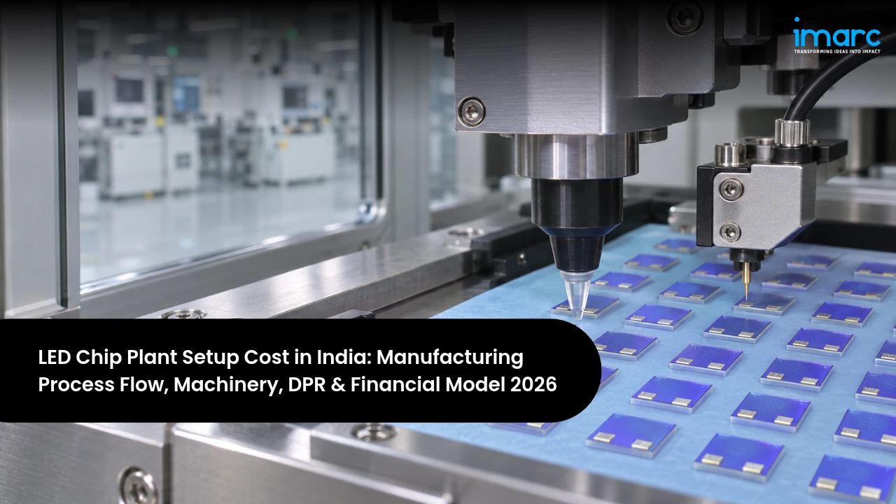
An LED Chip Manufacturing Plant Setup in India addresses one of the biggest gaps in the country's lighting and display supply chain. India assembles hundreds of millions of LED bulbs, battens, panels, and displays every year, yet almost all LED chips, the tiny semiconductor dies that actually emit light, are imported, mainly from China, Taiwan, and South Korea. An LED chip is made by growing thin layers of gallium nitride (GaN) or related compound semiconductors on a sapphire or other substrate, patterning them into millions of individual devices, and then dicing, testing, and packaging them. With the India Semiconductor Mission, PLI support for LED components, and rising demand from lighting, automotive, and display makers, domestic chip and package production is moving from ambition to early projects.
The overall LED Chip Manufacturing Plant Cost depends heavily on how much of the value chain the plant covers. An integrated front-end facility with epitaxy, chip processing, and testing for 50 to 100 million chips a month typically needs INR 300 crore to INR 700 crore, driven by MOCVD reactors, lithography and etch tools, and cleanrooms. A back-end packaging plant that buys LED wafers or dies and turns them into SMD or COB packages can start at around INR 40 crore to INR 100 crore. IMARC Group benchmarks for chip production point to gross margins of 40 to 50% and net margins of 15 to 20%, with raw materials at 40 to 50% and utilities at 30 to 35% of operating cost.
This guide is written for semiconductor and electronics companies, LED lighting and display makers, technology partners, and investors exploring how to start an LED Chip manufacturing plant in India. It explains chip types and applications, demand drivers, the epitaxy-to-package process, machinery and materials, site and utility planning, a detailed cost and returns breakdown, the approvals and incentives involved, and how a DPR pulls these elements into a bankable plan.
India Market Snapshot
| Key Facts | Details |
|---|---|
| Global LED Chip Market | USD 34.60 Billion (2025) |
| Global Market Outlook | USD 86.39 Billion by 2034, 10.7% CAGR |
| Indicative Total Investment | INR 300–700 Crore (integrated chip plant, 50–100 Million Chips/Month) |
| Typical Payback Period | 5–7 Years |
The snapshot shows a global market growing at double digits and an Indian market that IMARC Group expects to more than double by 2034, supported by lighting, backlighting, automotive, and display demand. Because nearly all of this demand is currently met by imports, local supply can tap a ready customer base. The investment range reflects the gap between a packaging-led entry and a full front-end plant with its own epitaxy and chip processing.
Investment Highlights
Indicative Project Cost in India (2026)
| Parameter | Value |
|---|---|
| Product Range | Blue and white lighting chips, red and green display chips, mid-power and high-power LED packages, mini LED |
| Total Project Investment | INR 300 – 700 Crore (integrated); INR 40 – 100 Crore (packaging only) |
| Payback Period | 5 – 7 Years |
| Net Profit Margin | 15 – 20% |
| IRR | 14 – 20% |
| Best Locations | Gujarat, Uttar Pradesh, Karnataka, Telangana, Tamil Nadu, Odisha |
| Mandatory Approvals | SPCB Consents, PESO Licenses (gases), Hazardous Chemical & Waste Compliance, Factory License, Fire NOC, GST |
| Key Requirement | Proven epitaxy and chip technology, stable power and ultrapure water, and anchor customers |
These figures offer a practical frame for early evaluation. Returns depend on licensing or developing competitive epitaxy and chip technology, reaching good yields quickly, securing reliable power, water, and specialty gases, accessing central and state semiconductor incentives, and signing offtake agreements with lighting, automotive, or display makers. A capacity- and technology-specific LED Chip Feasibility Report refines these numbers before capital is committed.
Table of Contents
- What is LED Chip Manufacturing?
- Why is LED Chip Manufacturing Growing in India?
- LED Chip Manufacturing Process Flow
- Raw Materials Required for LED Chip Manufacturing
- Location, Land & Infrastructure
- LED Chip Manufacturing Machinery and Equipment
- LED Chip Manufacturing Plant Setup Cost in India (CapEx & OpEx)
- Financial Analysis and Profitability
- Licenses and Approvals for LED Chip Manufacturing in India
- Recent Developments in the India LED Chip Manufacturing Industry
- How LED Chip Manufacturing Project Report and DPR Helps Investors
- Frequently Asked Questions
What is LED Chip Manufacturing?
LED chips are compound semiconductor devices. In a typical blue LED, layers of n-type GaN, indium gallium nitride quantum wells, and p-type GaN are grown on a patterned sapphire wafer by metal-organic chemical vapour deposition (MOCVD). The wafer is then processed with photolithography, etching, transparent conductive layers, and metal contacts, thinned, diced into thousands of tiny chips, and tested and sorted by wavelength and brightness. White LEDs are made by packaging blue chips with a yellow phosphor. An LED Chip Manufacturing Plant can therefore cover front-end epitaxy and chip fabrication, back-end packaging, or both.
Commercially, bare chips are sold to LED packaging companies, while packaged LEDs are sold to lighting, display, backlighting, automotive, and signage manufacturers. Buyers look for efficacy, wavelength and brightness consistency (tight binning), reliability, thermal performance, price, and assured supply, and automotive customers require additional qualification.
- Lighting Chips: Blue GaN chips used with phosphor to make white LEDs for bulbs, tubes, and luminaires.
- Display and Signage Chips: Red, green, and blue chips for video walls, signage, and fine-pitch displays.
- Backlighting and Mini LED: Small chips for TV, monitor, and laptop backlights and new mini LED displays.
- Automotive and Specialty Chips: High-reliability chips for headlamps and signals, plus infrared and UV devices.
Main Product Types in LED Chip Production
The product mix shapes technology choice, equipment, and margins:
| Product Type | Description | Key Feature | Primary Demand |
|---|---|---|---|
| Mid-Power Lighting Chips | Small blue GaN chips | High volume, low cost | General lighting packages |
| High-Power Chips | Larger, flip-chip or vertical designs | High current, good heat handling | Street, flood, industrial lights |
| RGB Display Chips | Red, green, and blue dies | Colour uniformity | Video walls, signage |
| Mini & Micro LED | Very small chips | Precision and high density | Premium displays, backlights |
| Packaged LEDs | SMD and COB packages | Ready for assembly | Lighting and display makers |
Most new entrants begin with packaging of mid-power and high-power LEDs, where technology is mature and demand is immediate, then move upstream into chip processing and epitaxy with a technology partner. Display, mini LED, and automotive chips offer higher value but need tighter process control, stronger R&D, and longer customer qualification.
Why is LED Chip Manufacturing Growing in India?
Key Growth Drivers in the Indian Market
Demand for locally made chips is driven by a large downstream industry and policy support for semiconductors.
- Large LED lighting industry: India's lighting makers assemble huge volumes of LED products but import almost all chips and packages.
- Semiconductor policy: The India Semiconductor Mission offers fiscal support for compound semiconductor fabs and packaging units, alongside state semiconductor policies.
- PLI for LED components: The PLI scheme for white goods covers LED chip packaging, drivers, and engines to raise domestic value addition.
- Displays and backlighting: Growth in LED video walls, signage, televisions, and mini LED displays adds demand for display chips.
- Automotive and smart lighting: Rising LED use in vehicles and connected lighting for smart cities drives higher-value chip demand.
India-Specific Market Opportunity
| Segment | India Market Context | Manufacturing Role |
|---|---|---|
| General Lighting | Very large assembly base | Mid-power chips and packages |
| Outdoor & Industrial Lighting | Street lighting and industrial projects | High-power chips and COB |
| Displays & Signage | Growing LED display assembly | RGB chips and packages |
| Consumer Electronics | TV and device assembly expanding | Backlight and mini LED chips |
| Automotive | Rising LED content in vehicles | Qualified high-reliability LEDs |
The strongest position for an LED Chip Manufacturing Plant in India begins with packaged LEDs for the domestic lighting industry, where customers are close and import substitution is clear, and builds towards chip processing, display chips, and automotive-grade products. Long-term supply agreements with large lighting and electronics groups reduce market risk during ramp-up.
LED Chip Manufacturing Process Flow
Understanding the LED Chip Manufacturing Process helps promoters plan technology, cleanroom layout, utilities, and yield management. Chip performance depends on epitaxial layer quality, defect density, uniformity across the wafer, accurate lithography and etching, good contacts, and careful testing and binning. The flow below reflects an integrated GaN-on-sapphire plant with optional packaging.
Step-by-Step LED Chip Manufacturing Process Flow
Patterned sapphire wafers are cleaned and loaded into MOCVD reactors, where GaN buffer, n-type, quantum well, and p-type layers are grown. Epi wafers are inspected, then patterned by photolithography and etched to form mesas, coated with transparent conductive and metal layers, passivated, thinned, and diced. Chips are probed, sorted, and binned, and may then be packaged with phosphor and encapsulant into SMD or COB devices.
| Unit Operation | Key Activity |
|---|---|
| Substrate Preparation | Clean patterned sapphire wafers |
| MOCVD Epitaxy | Grow GaN, quantum well, and p-GaN layers |
| Epi Wafer Inspection | Photoluminescence mapping, thickness, defects |
| Photolithography | Pattern mesa and contact areas |
| Etching | Dry etch to define chip structures |
| Transparent Layer & Metallisation | ITO layer and n- and p-contacts |
| Passivation & Thinning | Protective layers, back-grinding, polishing |
| Dicing | Laser scribing and breaking into chips |
| Probing, Sorting & Binning | Test and sort by wavelength and brightness |
| Packaging (Back-End) | Die attach, wire bond, phosphor, encapsulation, test, tape |
Two factors decide profitability. The first is yield: every wafer carries the cost of expensive reactors, gases, and cleanroom time, so uniform epitaxy, low defect density, and high usable chip output per wafer directly determine cost per chip. The second is binning and consistency: customers buy chips in tight wavelength and brightness bins, so the share of output landing in premium bins, together with reliability testing, decides average selling prices and customer loyalty.
Raw Materials Required for LED Chip Manufacturing
The main inputs are substrates, metal-organic sources, process gases, photoresists and chemicals, sputtering and evaporation materials, and, for packaging, lead frames, gold or alloy wire, phosphors, and encapsulants. Substrates and MO sources are the most important cost items for front-end production.
| Raw Material | Role in Process | India Sourcing | % of OpEx |
|---|---|---|---|
| Patterned Sapphire Substrates | Base wafer for GaN growth | Imported | 12–18% |
| MO Sources (TMGa, TMIn, TMAl) | Precursors for epitaxy | Imported specialty chemicals | 8–12% |
| Process Gases | Ammonia, hydrogen, nitrogen, silane | Domestic and imported high-purity gases | 6–10% |
| Photoresists, Chemicals & Targets | Lithography, etching, ITO, metals | Mostly imported | 8–12% |
| Packaging Materials | Lead frames, gold wire, phosphor, silicone | Imports and some domestic supply | 4–8% |
Almost all LED-specific materials are currently imported, so supplier qualification, inventory planning, and currency management are important. High-purity ammonia and hydrogen are consumed in large volumes in MOCVD and need on-site bulk storage or generation, while silane and other specialty gases require secure gas cabinets and monitoring. A front-end plant also needs ultrapure water and process chemicals in steady supply, which favours sites in emerging semiconductor clusters with shared infrastructure.
Location, Land & Infrastructure
Location shapes access to reliable power, water, specialty gases, skilled engineers, and customers. The best location for LED Chip manufacturing plant setup lies within a designated semiconductor or electronics cluster that offers stable high-voltage power, ultrapure water capability, gas suppliers, state semiconductor incentives, and good connectivity to LED lighting and electronics manufacturers.
Best Location for LED Chip Manufacturing Plant Setup in India
| State | Why It Works | Key Advantage |
|---|---|---|
| Gujarat | Dholera semiconductor region, Sanand packaging units | Semiconductor policy and infrastructure |
| Uttar Pradesh | Noida and Yamuna Expressway electronics clusters | Close to LED lighting makers |
| Karnataka | Bengaluru semiconductor design and electronics base | Engineering talent |
| Telangana | Hyderabad electronics and semiconductor push | Skilled workforce, state incentives |
| Tamil Nadu | Chennai electronics manufacturing belt | Strong supplier base and ports |
| Odisha | Emerging compound semiconductor projects | Land, power, and incentives |
Gujarat has emerged as India's leading semiconductor destination, with dedicated infrastructure and policy support, while Uttar Pradesh offers proximity to the largest concentration of LED lighting assemblers. Karnataka, Telangana, and Tamil Nadu bring engineering talent and electronics ecosystems, and Odisha is attracting compound semiconductor investment. For a packaging-only plant, being near customers matters most; for a front-end fab, utilities and incentives dominate the decision.
Quality, Safety and Environmental Requirements
Customers expect chips and packages with consistent wavelength, brightness, forward voltage, and reliability, supported by binning data, lifetime and stress testing, and quality systems such as ISO 9001, with IATF 16949 needed for automotive supply. The plant uses flammable and toxic gases such as hydrogen, ammonia, and silane, so gas detection, emergency shut-off, exhaust scrubbers, and trained emergency response are essential. Acid and solvent wastewater must be treated, hazardous wastes handled under authorisation, and cleanrooms maintained to strict particle and humidity limits.
Infrastructure Requirements (Integrated Chip Plant)
| Infrastructure Element | Specification | India-Specific Note |
|---|---|---|
| Total Land Area | 10 – 20 acres | Fab, utilities, gas yard, expansion |
| Cleanroom | ISO Class 5–7 areas | Lithography in the cleanest zones |
| Power Requirement | 8 – 20 MW | Dual feeders, UPS, backup generation |
| Ultrapure Water | On-site UPW plant | Continuous high-purity supply |
| Gas Systems | Bulk ammonia, hydrogen, nitrogen; gas cabinets | PESO norms, leak detection |
| Exhaust & Scrubbing | Toxic gas abatement, acid exhaust | SPCB consent conditions |
| Wastewater Treatment | Acid, fluoride, and ammonia treatment | Zero-discharge preferred |
Infrastructure for a chip plant centres on high-quality cleanrooms, uninterrupted power, ultrapure water, safe gas storage and distribution, effective exhaust abatement, and wastewater treatment. Reserving space for additional MOCVD reactors, a mini LED line, and a packaging block from the outset supports phased growth.
LED Chip Manufacturing Machinery and Equipment
LED chip equipment comes from a small number of specialised global suppliers, mainly in Germany, the United States, Japan, South Korea, and China. The main equipment is summarised below.
| Equipment | Function | Key Specification |
|---|---|---|
| MOCVD Reactors | Grow GaN epitaxial layers | Multi-wafer, high uniformity |
| Photoluminescence Mapper & XRD | Inspect epi wafers | Wafer-level mapping |
| Lithography Tools & Coater-Developer | Pattern wafers | Steppers or aligners with tracks |
| ICP Dry Etcher | Etch mesa and structures | Precise, uniform etching |
| PECVD System | Deposit passivation layers | SiO2 and SiN films |
| E-beam Evaporator & Sputter Tool | Deposit ITO and metal contacts | High-purity targets |
| Wafer Grinder & Polisher | Thin and polish wafers | Low damage |
| Laser Scriber & Breaker | Dice wafers into chips | High throughput |
| Prober & Sorter | Test and bin chips | Electro-optical testing |
| Packaging Line | Die bonder, wire bonder, dispenser, tester, taper | SMD and COB formats |
Equipment selection should follow the chosen technology, wafer size, and capacity. MOCVD reactors are the most expensive and capacity-defining tools, so technology partners often help size and tune them. Starting with packaging and test equipment, then adding chip processing and finally epitaxy, lets promoters build skills and customers step by step while spreading capital over time.
LED Chip Manufacturing Plant Setup Cost in India (CapEx & OpEx)
The tables below summarise the capital and operating cost structure of an integrated LED chip facility in India. The final LED Chip Investment Cost for a specific project depends on the value-chain scope, number of MOCVD reactors, wafer size, cleanroom area, utilities, technology licensing, and the incentives available.
Capital Expenditure (CapEx) Cost Structure
| CapEx Component | % of Total CapEx | What It Covers |
|---|---|---|
| Plant & Machinery | 55–65% | MOCVD, lithography, etch, deposition, test tools |
| Cleanroom & Facility Systems | 15–20% | Cleanroom, HVAC, UPW, gas delivery, scrubbers |
| Land & Buildings | 5–8% | Land and fab building |
| Technology & Training | 2–4% | Licensing, process transfer, engineer training |
| Pre-operative & Contingency | 3–5% | DPR, approvals, qualification runs |
| Working Capital | 6–10% | Substrates, MO sources, gases, receivables |
Equipment and cleanroom systems dominate the investment, which is why central and state semiconductor incentives can transform project economics. A packaging-only plant has a far lower capital requirement, with die bonders, wire bonders, dispensers, and testers forming most of the cost. An LED Chip Business Plan models these components so that scope, phasing, technology partnership, and financing rest on realistic numbers.
Operating Expenditure (OpEx) Cost Structure
| OpEx Component | % of Total OpEx | India-Specific Note |
|---|---|---|
| Raw Materials | 40–50% | Substrates, MO sources, gases, chemicals |
| Utilities | 30–35% | Power, UPW, cleanroom HVAC, nitrogen |
| Labour & Engineering | 6–9% | Process engineers, technicians, operators |
| Maintenance & Spares | 5–7% | Reactor parts, pumps, consumables |
| Overheads & Compliance | 2–4% | Safety, testing, environmental compliance |
Utilities are unusually large because cleanrooms, MOCVD reactors, and ultrapure water run around the clock. Profitability therefore depends on industrial power tariffs, yields, reactor uptime, and material prices. A sound financial model should test margins against chip price declines, yield ramp-up, power costs, and capacity utilisation, and for packaging-only plants against the cost of purchased dies.
Financial Analysis and Profitability
LED chips can deliver solid long-term returns, but they require patient capital and strong technical execution. The profitability of LED Chip manufacturing business in India improves with fast yield ramp-up, high reactor utilisation, a richer mix of high-power, display, and automotive chips, available semiconductor incentives, and secure offtake from domestic lighting and electronics makers.
| Financial Metric | Indicative Value | India Context |
|---|---|---|
| Gross Profit Margin | 40–50% | Higher for display, mini LED, and automotive chips |
| Net Profit Margin | 15–20% | After depreciation and Indian corporate taxes |
| Payback Period | 5–7 Years | High capital intensity, faster with incentives |
| IRR (Internal Rate of Return) | 14–20% | Sensitive to yields and chip prices |
| Capacity Utilization (stable ops) | 70–90% | After yield ramp-up |
| Break-even Capacity Utilization | 50–65% | High fixed costs |
Scale, yield, and pricing are the decisive factors. Global LED chip prices are under constant pressure from large Chinese producers, so a new Indian plant must reach competitive yields quickly, focus on segments where local supply and quality matter, and use incentives to offset its scale disadvantage. Packaging plants earn lower margins than the benchmark but need much less capital and can be profitable sooner.
Returns can be strengthened by partnering with an experienced epitaxy and chip technology provider, phasing investment from packaging to chip processing to epitaxy, locating in a semiconductor cluster with shared utilities, securing ISM and state support, signing long-term supply agreements with lighting and display makers, and targeting display, mini LED, and automotive segments.
Key Risks and Mitigation
The main risks are technology and yield risk, intense global price competition, dependence on imported materials and equipment, utility interruptions, rapid technology change towards mini and micro LED, long customer qualification, and gas and chemical hazards. Technology risk is reduced through proven partners and experienced teams; price risk through segment focus and incentives; supply risk through dual sourcing and inventory buffers; utility risk through redundant power and water systems; technology change risk through flexible tools and R&D; and safety risk through robust gas and chemical management.
Licenses and Approvals for LED Chip Manufacturing in India
An LED chip plant requires environmental, hazardous materials, industrial, and incentive-related approvals. Promoters typically need the following before commencing operations:
- Pollution Control Consents: Consent to Establish and Consent to Operate from the State Pollution Control Board, along with environmental clearance where applicable.
- PESO Licenses: Licenses for storing hydrogen, ammonia, and other compressed or liquefied gases under the applicable gas cylinder and pressure vessel rules.
- Hazardous Chemical and Waste Compliance: Safe storage and handling of toxic and flammable chemicals, an on-site emergency plan, and hazardous waste authorisation.
- Factory License and Fire NOC: Factory registration, building plan approval, and fire safety approval for cleanrooms and gas areas.
- Semiconductor Incentive Approvals: Approval under the India Semiconductor Mission or the PLI scheme for LED components, and state semiconductor policy incentives, where applied for.
- Quality Certifications: ISO 9001, ISO 14001, and IATF 16949 for automotive customers.
- Business, Tax and Labour Registrations: Company incorporation, GST, Udyam, an Import Export Code for equipment and material imports, and EPF and ESI registrations.
Pollution consents, gas licenses, and incentive approvals sit on the critical path for most projects, while customer qualification and quality certifications should be planned alongside construction. Engaging an LED Chip Manufacturing Consultant in India can help promoters choose the right value-chain scope, identify technology partners, plan approvals and incentive applications, and design utilities and safety systems.
Note: The exact approvals, registrations, licenses, and certification requirements may vary depending on factors such as plant location, product range, capacity, target customers, and applicable regulations. Businesses are advised to undertake a detailed regulatory assessment during the project planning stage to ensure full compliance and timely implementation.
Recent Developments in the India LED Chip Manufacturing Industry
Several recent developments are shaping LED chip production in India and the wider region:
- First mini and micro LED fab approved: In May 2026, the Union Cabinet approved Crystal Matrix's GaN-based mini and micro LED display facility at Dholera, Gujarat, under the India Semiconductor Mission, with a Korean epitaxy partner and an annual target of 72,000 square metres of display panels and 24,000 RGB wafer sets. It was approved alongside a semiconductor packaging unit, with the two projects together valued at about USD 414 million.
- PLI support for LED components: A January 2026 update on the PLI scheme for white goods reported 85 selected companies across air conditioner and LED components with cumulative committed investment of INR 11,198 crore. Supported LED components include chip packaging, drivers, engines, and light management systems.
- Regional packaging competition: In August 2025, Chinese LED supplier Azure announced a USD 83.9 million LED chip packaging plant in Malaysia, planned at 700 million units a month, showing the scale at which Asian competitors are expanding packaging capacity outside China.
Together these point to early government-backed compound semiconductor projects in India, continued incentives for LED component localisation, and intense regional competition. For new entrants, success depends on a credible technology partner, phased investment, strong yields, and secure domestic offtake.
How LED Chip Manufacturing Project Report and DPR Helps Investors
A detailed LED Chip Project Report gives investors a structured roadmap covering market demand by chip type and application, value-chain scope, technology options, process design, machinery, cleanroom and utility layout, materials sourcing, safety and environmental systems, regulatory pathway, incentives, and economics. It helps promoters choose the right scope, phasing, and capacity, estimate capital expenditure (CapEx) and operating expenditure (OpEx), assess profitability, and identify risks before implementation.
At the core of the DPR is an LED Chip Financial Model covering wafer starts, yields, chips per wafer, bin distribution, selling prices, material and utility costs, incentive flows, working capital, cash flow projections, break-even, return on investment (ROI), and payback. Because returns hinge on yield ramp-up and price trends, lenders expect detailed sensitivity analysis, which is why many promoters engage an LED Chip Plant Project Report Consultant in India to prepare bank-ready documents.
For an LED chip project specifically, a strong DPR also answers the questions that matter most: whether to start with packaging or go straight to chip fabrication, which technology partner to work with, how quickly yields can reach competitive levels, how incentives will be accessed, and how returns hold up when global chip prices fall. An experienced LED Chip Manufacturing Feasibility Study Consultant tests these scenarios so that the final plan is one lenders and partners can back with confidence.
Frequently Asked Questions
How do I set up an LED chip manufacturing unit in India?
Start by defining the value-chain scope and target customers, then commission a feasibility study and DPR. Choose a technology partner, select a site in a semiconductor or electronics cluster, apply for central and state incentives, build cleanrooms and utilities, install equipment, obtain pollution, gas, chemical, factory, and fire approvals, and run qualification batches with customers before volume production.
What is the LED chip manufacturing plant setup cost in India?
An integrated plant with epitaxy, chip processing, and testing for 50 to 100 million chips a month typically needs INR 300 crore to INR 700 crore, while a packaging-only plant can start at around INR 40 crore to INR 100 crore, depending on capacity, technology, and utilities.
How are LED chips made?
GaN layers are grown on sapphire wafers by MOCVD, then patterned by photolithography, etched, coated with transparent and metal contacts, passivated, thinned, and diced into chips. Chips are tested and binned by wavelength and brightness and may be packaged with phosphor and encapsulant.
What machinery is needed for an LED chip manufacturing plant?
Key equipment includes MOCVD reactors, photoluminescence mappers, lithography tools and coater-developers, ICP etchers, PECVD systems, e-beam evaporators and sputter tools, wafer grinders, laser scribers, probers and sorters, and a packaging line with die bonders, wire bonders, dispensers, and testers.
What raw materials are used in LED chips?
The main inputs are patterned sapphire substrates, metal-organic sources such as TMGa and TMIn, ammonia, hydrogen, nitrogen, and silane, photoresists, chemicals, and ITO and metal targets, plus lead frames, gold wire, phosphors, and encapsulants for packaging.
Is LED chip manufacturing profitable in India?
A well-run integrated plant can earn a 15 to 20% net margin and an IRR of around 14 to 20%, with payback in 5 to 7 years. Profitability depends on yields, scale, chip prices, power costs, and access to semiconductor incentives.
What licenses are needed for an LED chip manufacturing unit in India?
A unit typically needs State Pollution Control Board consents, PESO licenses for gases, hazardous chemical and waste compliance, a Factory License, a Fire NOC, quality certifications, incentive approvals where applied for, and GST, Udyam, and labour registrations.
Which state is best for an LED chip manufacturing plant?
Gujarat, Uttar Pradesh, Karnataka, Telangana, Tamil Nadu, and Odisha are strong options. The best site offers stable power and water, semiconductor incentives, gas supply, skilled engineers, and access to LED lighting and electronics customers.
How do I get a feasibility study or DPR for an LED chip manufacturing plant?
A professionally prepared DPR covers market assessment, technology and scope selection, sourcing, technical design, approvals, incentives, costs, and financial projections for bank appraisal. Many promoters work with an LED Chip Business Plan Consultant in India to prepare it and align it with lender requirements.
Our Clients










Contact Us
Have a question or need assistance?
Please complete the form with your inquiry or reach out to us at
Phone Number
+91-120-433-0800+1-201-971-6302
+44-113-547-7077
Previous Post

A Smartphone Manufacturing Plant Setup in India places an investor inside one of the country's biggest industrial success stories of the past decade.
A Smart Watch Manufacturing Plant Setup in India serves one of the world's largest wearables markets. Indian consumers buy tens of millions of smartwatches every year, and domestic brands have shifted much of their production from imports to local contract manufacturers.
The India Semiconductor Market has moved past the stage of ambition documents and into the stage of concrete assets, approved sites and dated delivery milestones. The India Semiconductor Market size reached USD 59.78 Billion in 2025, expanded to USD 73.00 Billion in 2026, and is projected to reach USD 180.20 Billion by 2034, growing at a CAGR of 11.95% over the 2026-2034 forecast period.
A genset combines an engine, usually diesel or gas, with an alternator that converts its motion into electricity, mounted on a steel base frame with a fuel tank, exhaust and emission after-treatment, a control panel, and in most cases a soundproof acoustic enclosure.
Setting up a Power Cable Manufacturing Plant in India puts an investor directly in the path of one of the country's largest infrastructure build-outs.
Servos are precision electric motors fitted with a position sensor, called an encoder, and paired with an electronic drive that controls speed, torque, and position very accurately.
PVC-insulated wires and cables are made by drawing copper or aluminium rod into fine conductors, annealing and stranding them, and covering them with coloured PVC insulation and, for multi-core cables, an outer PVC sheath and sometimes steel armour.
Portable chargers are compact battery packs made from lithium-ion or lithium-polymer cells, a charging and protection circuit board, ports or wireless coils, and a plastic or metal casing.
Small electric cooking and food preparation products, such as mixer grinders, induction cooktops, electric kettles, air fryers, hand blenders, and sandwich makers, are made by moulding plastic bodies, forming steel and aluminium parts, winding motors or fitting heating elements, assembling control boards, and wiring and testing each unit for safety.
Aluminum-air batteries generate electricity by reacting aluminum plates with oxygen from the air in a water-based electrolyte. Aluminum has a very high theoretical energy density, and instead of being recharged from a socket, spent plates are swapped for fresh ones while the aluminum hydroxide produced is recycled into new aluminum.
LED bulbs use light-emitting diodes mounted on a metal-core circuit board, powered by a small electronic driver and housed in a plastic and aluminium body with a diffuser and a standard B22 or E27 cap.
Inverters convert direct current from batteries or solar panels into the alternating current used by homes, shops, and factories.
Electrical control panels are steel enclosures that house circuit breakers, contactors, relays, busbars, meters, drives, and controllers to distribute power and control motors, machines, and processes safely.
Microchips, or integrated circuits and semiconductor devices, are the building blocks of phones, computers, vehicles, appliances, power systems, telecom networks, and defence equipment.
Resistors are the most widely used electronic components, found by the dozens or hundreds in almost every circuit board, from phones, laptops, and televisions to vehicles, appliances, telecom equipment, power electronics, medical devices, and defence systems.
Rare earth magnets, mainly neodymium-iron-boron (NdFeB) and samarium-cobalt, are the strongest permanent magnets made, and they sit at the heart of electric vehicle motors, wind turbine generators, electronics, industrial automation, medical devices, and defence systems. India imported over 53,000 tonnes of rare earth permanent magnets in 2024-25 and has almost no domestic production, while demand is expected to double by 2030.
Wires and cables carry power and signals through every home, office, factory, railway, data centre, and solar park, and India's market has grown to about USD 10 billion as construction, power transmission, renewable energy, and industrial investment have expanded.
Heat exchangers are among the most widely used pieces of engineering equipment in the world. Refineries, petrochemical and fertiliser plants, power stations, pharmaceutical and food factories, HVAC systems, and data centers all depend on them to heat, cool, condense, and recover energy from process streams.
India's trucks and buses rarely rest. They carry freight across highway corridors, move goods from ports and factories, and ferry millions of passengers every day, often under heavy loads and tough road conditions.
Silicon wafers are the thin, precisely sliced discs and squares on which solar cells and computer chips are built. India has rapidly become a major assembler of solar modules and is now building cell capacity, but almost all of the wafers those cells need are still imported.
Every video call, UPI payment, and 5G connection in India ultimately travels over glass. Fiber optic cables carry the country's data between cities, into mobile towers and data centres, and increasingly right into homes through fiber-to-the-home connections.
Setting up an Air Conditioner Manufacturing Plant in India is an assembly-driven, high-volume consumer durable venture, powered by rising household incomes, extreme summers, rapid urbanisation, and one of the lowest room air-conditioning penetration rates among large economies.
Setting up a High Voltage Cable Manufacturing Plant in India is a capital-intensive, high-value venture, powered by the country's massive power-transmission expansion, renewable-energy build-out, and the shift toward underground cabling in cities.
Setting up a Copper Cable Manufacturing Plant in India is a high-demand, infrastructure-driven venture, powered by the country's construction boom, rapid electrification, and steady industrial and appliance demand.
Setting up a Junction Box Manufacturing Plant in India is a high-demand, infrastructure-driven venture, powered by the country's construction boom, rapid electrification, and expanding solar and industrial sectors.
Setting up an Electric Cable Manufacturing Plant in India is a high-demand, infrastructure-linked venture, powered by the country's rapid growth in power, construction, renewable energy, and electrification. Cables and wires are essential to every building, factory, grid, and vehicle, giving an Electric Cable Manufacturing Plant a large and steadily growing market.
Setting up a Semiconductor Fabrication Manufacturing Plant in India is a highly capital-intensive but strategically transformative venture, driven by the country's semiconductor mission, deep policy incentives, and a vast import-substitution opportunity. Semiconductors are the foundation of every modern electronic and digital product, yet India currently imports almost all of its chip requirement.
Setting up a PCB Manufacturing Plant in India is a capital-intensive but strategically timed venture, driven by the country's electronics manufacturing push, strong policy incentives, and a large import-substitution opportunity. Printed circuit boards are the backbone of every electronic product, yet India still imports the overwhelming majority of its PCB requirement.
The Indian PCB (Printed Circuit Board) Market is emerging as the physical backbone of the country's electronics manufacturing ambitions. The market reached USD 7.27 Billion in 2025 and is projected to reach USD 25.48 Billion by 2034, growing at a CAGR of 14.96% (2026–2034), a total addressable market expansion driven by the Production Linked Incentive (PLI) scheme, 5G infrastructure rollout, and rising domestic consumer electronics demand.
Setting up an E-waste Recycling Plant in India is a capital-intensive but high-potential venture, driven by the country's soaring volume of discarded electronics, tightening Extended Producer Responsibility regulations, and the rising value of recovered metals. India is now among the world's largest generators of electronic waste, yet only a small share is processed through formal, compliant channels, leaving a large, policy-backed opportunity for organized recyclers who can capture volumes shifting from the informal sector.
Global semiconductor demand across automotive, data centers, and defense, highlighting market segmentation, key applications, regional dynamics, and industry shifts.
The hearables market represents one of the most dynamic segments within consumer electronics and wearable technology. These intelligent audio devices have evolved beyond simple wireless earbuds into multifunctional platforms combining premium audio with health monitoring, artificial intelligence, and seamless digital connectivity.
A smart washing machine is a sophisticated home appliance that incorporates advanced digital features such as connectivity, sensor technology, and automated controls for improved efficiency, convenience, and user control. In contrast to traditional washing machines, smart washing machines come pre-installed with advanced features such as Wi-Fi connectivity, smart load detection, smart detergent dispensing, and voice-control capability.
A smartphone is a portable electronic device that combines sophisticated capabilities in computer processing, wireless communication, multimedia entertainment, and internet access. Smartphones are distinct from other mobile phones in that their operation involves highly sophisticated platforms of operation that are capable of supporting multiple applications, multitasking, and connectivity with internet platforms.
Semiconductor manufacturing is a highly specialized industrial process that involves the design, fabrication, and assembly of semiconductor devices including integrated circuits (ICs), memory chips, sensors, and discrete components. The process transforms raw semiconductor materials, primarily silicon, into sophisticated electronic components through a combination of physical and chemical processing steps, such as wafer fabrication, photolithography, doping, etching, thin-film deposition, and packaging.
The retail landscape is experiencing a profound transformation as self-checkout systems emerge as critical infrastructure components reshaping consumer experiences and operational efficiency globally. These automated solutions enable customers to independently scan, bag, and pay for purchases without cashier assistance, representing a fundamental shift in modern commerce.
The webcams market is experiencing unprecedented transformation as digital communication becomes the cornerstone of modern business, education, and healthcare. Global webcam industry dynamics are being reshaped by technological innovation and evolving workplace models.
As smartphones become a way of life for most Filipinos, the market has changed dramatically and expectations from consumers are higher than ever before. With the demand for smartphones growing, there is a significant change in consumer shopping habits with more emphasis on using online platforms for shopping. This change is closely interlinked with the fast growth of the Philippines e-commerce market, both bringing opportunities and challenges to the stakeholders of the smartphone industry.
As technology continues to advance, lighting has transformed from a basic necessity into a strategic enabler of innovation, efficiency, and sustainability. The evolution from incandescent bulbs to LEDs, smart systems, and intelligent lighting networks represents not just technological change but a redefinition of how energy, design, and functionality intersect in the built environment.
An LED light is an illuminating device that utilizes Light Emitting Diodes as its source of light, generating light through a semiconductor-based process called electroluminescence. When electrical current flows across the semiconductor material of the diode, electrons emit energy as photons and thus produce highly efficient and concentrated illumination.
An LED bulb is a solid-state lighting device that uses Light Emitting Diodes (LEDs) as its illumination source. Different from incandescent or fluorescent lamps, light in LED bulbs is produced by electroluminescence, a process where the passing of an electric current through a semiconductor material emits photons directly. This process is highly energy-efficient, with a far larger percentage of the electricity being converted to usable light and very little heat generated in the process.
The junction box, generally made from plastic, metal, or composite materials, houses wire connections, terminations, and protective components to allow the safe distribution and routing of electrical circuits. The junction box will provide insulation, mechanical protection, and a secure environment to avoid accidental contact with live electrical parts, moisture intrusion, or dust accumulation.
The Japan power electronics market is poised to grow substantially, driven by rising demand in automotive, energy, industrial automation, and infrastructure sectors. According to IMARC Group, the Japan power electronics market is studied from 2019 to 2024 with projections extending to 2033.
Japan's printed circuit board (PCB) industry is the world leader in technology innovation, enabling consumer electronics, automotive, and next-generation communication system development. As a key enabler of modern electronic products, PCBs provide the essential building blocks for embedding semiconductors, sensors, and microchips into miniaturized, high-performance devices. Japan, through its world-class manufacturing base and engineering expertise, remains the hub of the global PCB supply chain.
Aluminum-Air (Al-Air) battery is a new energy storage technology that has attracted interest as a future alternative to conventional lithium-ion batteries, specifically for electric vehicle (EV) use. As opposed to normal rechargeable batteries, the Al-Air battery is a metal-air electrochemical cell with aluminum as the anode, oxygen from the ambient air as the cathode reactant, and a liquid electrolyte (commonly sodium hydroxide or potassium hydroxide) as the medium through which the reaction occurs.
Aluminium wire is an essential industrial commodity commonly employed in power transmission, electrical distribution, building construction, and manufacturing processes owing to its high conductivity-to-weight ratio, resistance to corrosion, and cost advantage over copper. Produced by methods including continuous casting, rolling, and drawing, aluminum wire is available in various grades and alloys to serve the wide demands, from overhead transmission conductors and building wiring to automotive harnesses and electronic applications.
Air conditioners are electromechanical devices used to control indoor climate by extracting heat and humidity and ensuring optimum air circulation. Generally consisting of a compressor, condenser, evaporator, refrigerant fluid, filters, fans, and electronic controls, air conditioners work based on the principle of heat exchange, moving heat from indoor areas to the external environment. Contemporary units come in diverse configurations, such as split systems, window units, central air systems, and portable models, supporting respective residential, commercial, and industrial applications. Some of the major characteristics are efficiency in cooling, energy use, noise rating, and environmental footprint in relation to refrigerant type.
E-waste, or electronic waste, is electrical and electronic equipment that has been discarded, such as computers, cell phones, television sets, servers, and household appliances. It is among the world's fastest-growing streams of waste, consisting of a heterogeneous combination of metals, plastics, glass, and toxic substances. E-waste contains valuable metals like copper, aluminum, gold, silver, palladium, and rare earth elements, in addition to toxic materials like lead, mercury, cadmium, and brominated flame retardants.
Polished silicon wafers are very pure, ultra-flat semiconductor substrates that are produced from high-quality single-crystal silicon. The wafers act as the material base for making integrated circuits, power devices, and MEMS (Microelectromechanical Systems). The wafers are made of monocrystalline silicon ingots using the Czochralski or Float-Zone process, from which the wafers are cut, lapped, etched, and polished to atomic-scale flatness and defect-free surfaces.
AI is revolutionizing Japan’s semiconductor industry by boosting innovation and efficiency across the entire value chain. Advanced artificial intelligence (AI)-powered Electronic Design Automation (EDA) tools significantly shorten chip design cycles, improving performance and energy efficiency.
Recent projections indicate that Australia semiconductor market, including services, is growing at a steady compound annual growth rate as the nation deepens its tech infrastructure. The importance of semiconductors spans electronics, defense systems, telecommunications, and emerging AI applications, which position the local ecosystem as strategically vital for growth.
Fiber optic cables are high-tech communications cables that carry information like bursts of light along extremely thin glass or plastic strands, providing high-speed, high-bandwidth connectivity with little loss of signal. Fiber optic cables make up the foundation of contemporary telecommunications, carrying internet, cloud computing, 5G networks, and smart infrastructure.
CAT (Category) cables are twisted-pair Ethernet cables utilized for copper-based wired network communications, varying from CAT5e to CAT8 standards. The cables carry data through copper conductors, but with different speeds (up to 40 Gbps for CAT8) and bandwidths, supporting networks such as LANs, data centers, and smart buildings.
India's semiconductor industry is undergoing a revolutionary phase driven by rising demand from industries like consumer electronics, automotive technologies, industrial automation, and telecom infrastructure.
USB data cables are critical elements of contemporary digital connectivity, enabling high-speed and consistent data transfer and power supply for a broad scope of electronic products. They provide the foundation for charging and synchronizing smartphones, tablets, laptops, and other peripherals, with significant applications in consumer electronics, industrial automation, and new technologies. With technologies like USB-C, the cables today carry faster data speeds, more power output, and universal compatibility, making them essential in a world that is connected.
Thin-film-transistor (TFT) liquid-crystal display (LCD) is a type of display technology used in many electronic devices, such as smartphones, tablets, laptops, and televisions (TVs). A backlight, colour filters, a thin-film transistor array, and a liquid crystal layer are among the layers that make up this flat-panel display. TFT LCDs are made to produce sharp images with superb viewing angles, strong contrast, and accurate colour reproduction. They are made up of thousands of tiny transistors that regulate how much light enters each pixel. This makes it possible for the display to generate crisp, detailed images at rapid refresh rates. TFT LCD technology's low power consumption is one of its main benefits, which makes it perfect for battery-operated gadgets.
Polycrystalline solar photovoltaic (PV) modules are a key component of solar energy systems, harnessing sunlight and converting it into electricity through the photovoltaic effect. These modules are composed of multiple interconnected solar cells, each made from polycrystalline silicon. Polycrystalline solar panels are renowned for their efficiency, affordability, and versatility, making them a popular choice for various applications such as solar installations, commercial and industrial projects, off-grid systems and solar farms.
The LED chip is the core component of an LED bulb, comprising semiconductor layers that enable the free flow of protons and electrons. Employed in all LED lighting fixtures—from bulbs to tubes—the LED chip fundamentally determines light quality, with variations in brightness, voltage, and wavelength. These chips are manufactured through a process called MOCVD (metal-organic chemical vapor deposition), which creates the semiconductor layers that facilitate electric flow. Major applications of these chips include backlighting, illumination, automotive lighting, signs, and signals.
Semiconductors are crucial components in the modern electronics industry, used in electronic equipment and devices to manage and control the flow of electricity. They are found in consumer items like smartphones, wearables, smart TVs, and advanced equipment used in industrial applications, defense, and aerospace. Semiconductors are further divided into four broad categories: optoelectronics, discrete components, integrated circuits, and sensors. Memory devices, logic devices, analog ICs, MPUs, discrete power devices, MCUs, and sensors are some of the major components of semiconductors.